Method for forming bump of semiconductor package

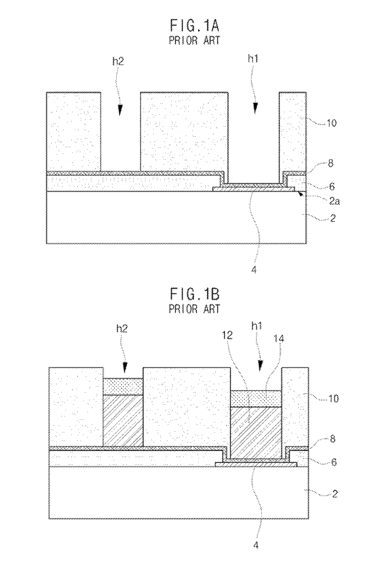
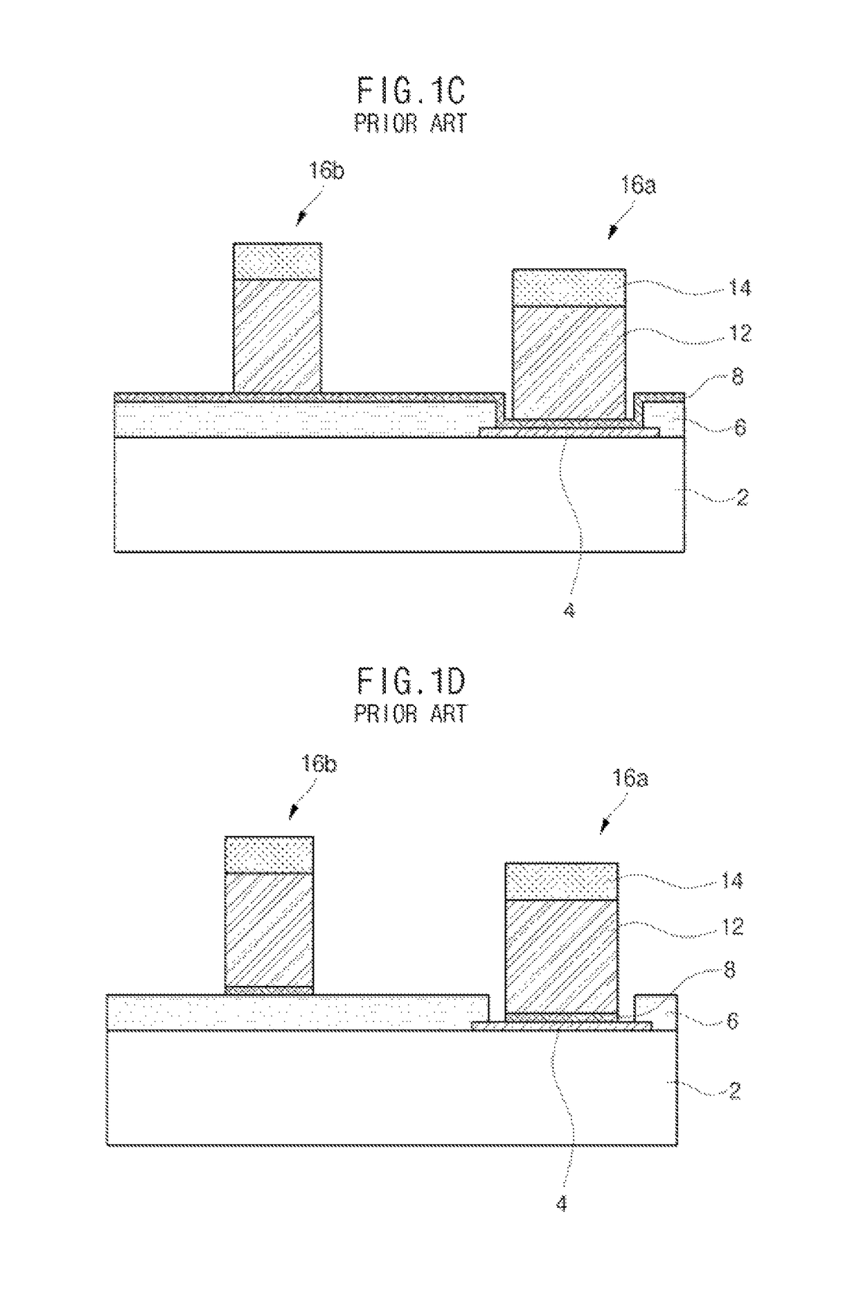
a semiconductor and packaging technology, applied in semiconductor devices, semiconductor/solid-state device details, electrical apparatus, etc., can solve the problems of reducing the physical coupling force between the semiconductor chip and the printed circuit board, affecting the final height of the bump, and affecting the appearance of the packag

Active Publication Date: 2018-07-24
SMART MODULAR TECH LX S A R L
View PDF14 Cites 7 Cited by
  • Summary
  • Abstract
  • Description
  • Claims
  • Application Information

AI Technical Summary

Benefits of technology

[0021]In an embodiment, there is provided a method for forming bumps of a semiconductor package to suppress a final height difference between main bumps and support bumps that is caused by a height difference between areas of an underlying layer when viewed on a cross-section. The method may include forming first seed layer patterns and second seed layer patterns which are disposed in the areas and are separated from each other, over the underlying layer having the height difference. The method may include forming the main bumps and the support bumps of which final heights are the same when viewed on the cross-section in the areas, by performing electroplating through using, as electrodes, the first seed layer patterns and the second seed layer patterns which are disposed in the areas and are separated from each other, under different conditions in the areas.

Problems solved by technology

However, in the conventional art for forming bumps, a difference exists in the final heights of the bumps due to a difference in the heights of an underlying layer.
Owing to this fact, when flip-chip bonding a semiconductor chip, as a main bump is not brought into contact with a bond finger of a printed circuit board, an electrical connection may not be appropriately formed, and a physical coupling force between the semiconductor chip and the printed circuit board may decrease.

Method used


Image

  • Method for forming bump of semiconductor package
  • Method for forming bump of semiconductor package
  • Method for forming bump of semiconductor package

Examples


Embodiment Construction

[0028]Various embodiments may provide a method for forming bumps of a semiconductor package, capable of controlling the final heights of the bumps to be uniform, while not decreasing a bonding force between the semiconductor chip and the bumps. Also, various embodiments may provide a method for forming bumps of a semiconductor package, capable of securing bonding reliability in flip-chip bonding of the semiconductor chip by uniformizing the final heights of the bumps even with a height difference of layers lying under the bumps.

[0029]Hereinafter, a method for forming bumps in a semiconductor package will be described below with reference to the accompanying drawings through various examples of embodiments.

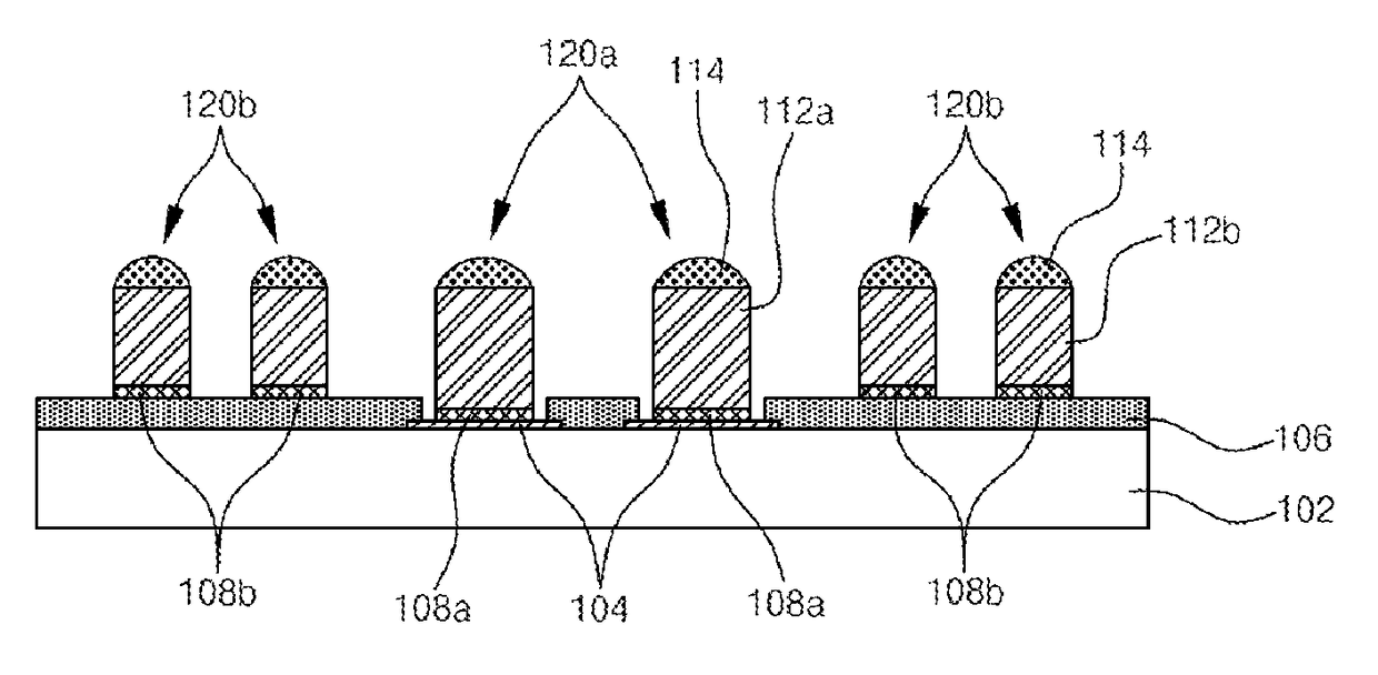
[0030]FIGS. 5A to 5I are representations of examples of cross-sectional views by processes to assist in the explanation of a method for forming bumps of a semiconductor package in accordance with an embodiment.

[0031]Referring to FIG. 5A, a semiconductor chip 102 in which an integra...


PUM


Abstract

The present invention provides a method for forming bumps of a semiconductor package to suppress a final height difference between main bumps and support bumps that is caused by a height difference between areas of an underlying layer when viewed on a cross-section. The method may include forming first seed layer patterns and second seed layer patterns which are disposed in the areas and are separated from each other, over the underlying layer having the height difference. The method may include forming the main bumps and the support bumps of which final heights are the same when viewed on the cross-section in the areas, by performing electroplating through using, as electrodes, the first seed layer patterns and the second seed layer patterns which are disposed in the areas and are separated from each other, under different conditions in the areas.

Description

CROSS-REFERENCE TO RELATED APPLICATION[0001]The present application claims priority to Korean Patent Application No. 10-2016-0171482 filed on Dec. 15, 2016, in the Korean Intellectual Property Office, which is incorporated herein by reference in its entirety.BACKGROUND1. Technical Field[0002]The present invention generally relate to a method for manufacturing a semiconductor package, and more particularly, to a method for forming bumps of a semiconductor package for flip-chip bonding.2. Related Art[0003]With the development of the information communication and digital technologies, demands for new materials, semiconductor parts and modules, and substrates which are used in high frequency regions and have high data processing speeds are increasing. Also, according to trends toward the miniaturization, multiple bands and high frequency of mobile communication terminals, the high frequency, high degree of integration and miniaturization of semiconductor parts are being demanded.[0004]K...

Claims


Application Information

Patent Timeline
Patent Type & Authority Patents(United States)
IPC IPC(8): H01L23/00
CPCH01L24/11H01L2224/11462H01L2924/01029H01L2224/14517H01L2924/014H01L2224/1401H01L21/4853H01L23/49816H01L24/03H01L24/05H01L24/06H01L24/13H01L24/14H01L2224/0345H01L2224/03462H01L2224/036H01L2224/0401H01L2224/05018H01L2224/05023H01L2224/05024H01L2224/05073H01L2224/05552H01L2224/05558H01L2224/05559H01L2224/05568H01L2224/05569H01L2224/06051H01L2224/06102H01L2224/1147H01L2224/11849H01L2224/119H01L2224/13006H01L2224/13022H01L2224/13023H01L2224/13082H01L2224/131H01L2224/1403H01L2224/14051H01L2924/00014H01L2924/00012H01L2224/11845H01L21/0274H01L21/288H01L23/488H01L24/12
Inventor PARK, BUM WOOKJUNG, HYUN
Owner SMART MODULAR TECH LX S A R L
Why Eureka
Try Eureka