Porosity measurement of semiconductor structures

a technology of porous structure and semiconductor, applied in the field of porous structure measurement, can solve the problems of unsuitable production environment, unsuitable techniques, and undesirable high-volume manufacturing, and achieve the effect of enhancing measurement contras

Active Publication Date: 2018-08-07
KLA CORP
View PDF51 Cites 6 Cited by
  • Summary
  • Abstract
  • Description
  • Claims
  • Application Information

AI Technical Summary

Benefits of technology

[0012]In another aspect, model based measurements of porosity are performed with a data set including measurement signals collected from a metrology target having geometric features filled with a condensate. The presence of the condensate changes the optical properties of the structure under measurement compared to a measurement scenario where the purge gas is devoid of any fill material.
[0013]In some examples, multiple measurements of a metrology target are performed for different adsorption states. Each measurement corresponds to a different amount of condensate condensed onto the structures under measurement. By collecting measurement signal information associated with a metrology target having geometric features filled with different amounts of condensate, parameter correlation among floating measurement parameters is reduced and measurement accuracy is improved.
[0018]In some embodiments, the fill material exhibits fluorescence in response to the illumination light provided to the structures under measurement to enhance measurement contrast, particularly in image based measurement applications.

Problems solved by technology

The porosity of films used in the manufacture of semiconductor devices significantly impacts device performance.
Unfortunately, these techniques are unsuitable for production environments.
Unfortunately, these measurements are generally performed in a high-vacuum environment, which is suitable as a laboratory reference technique, but is undesirable for high-volume manufacturing.
Future metrology applications present challenges due to increasingly small resolution requirements, multi-parameter correlation, increasingly complex geometric structures, and increasing use of opaque materials.

Method used


Image

  • Porosity measurement of semiconductor structures
  • Porosity measurement of semiconductor structures
  • Porosity measurement of semiconductor structures

Examples


Embodiment Construction

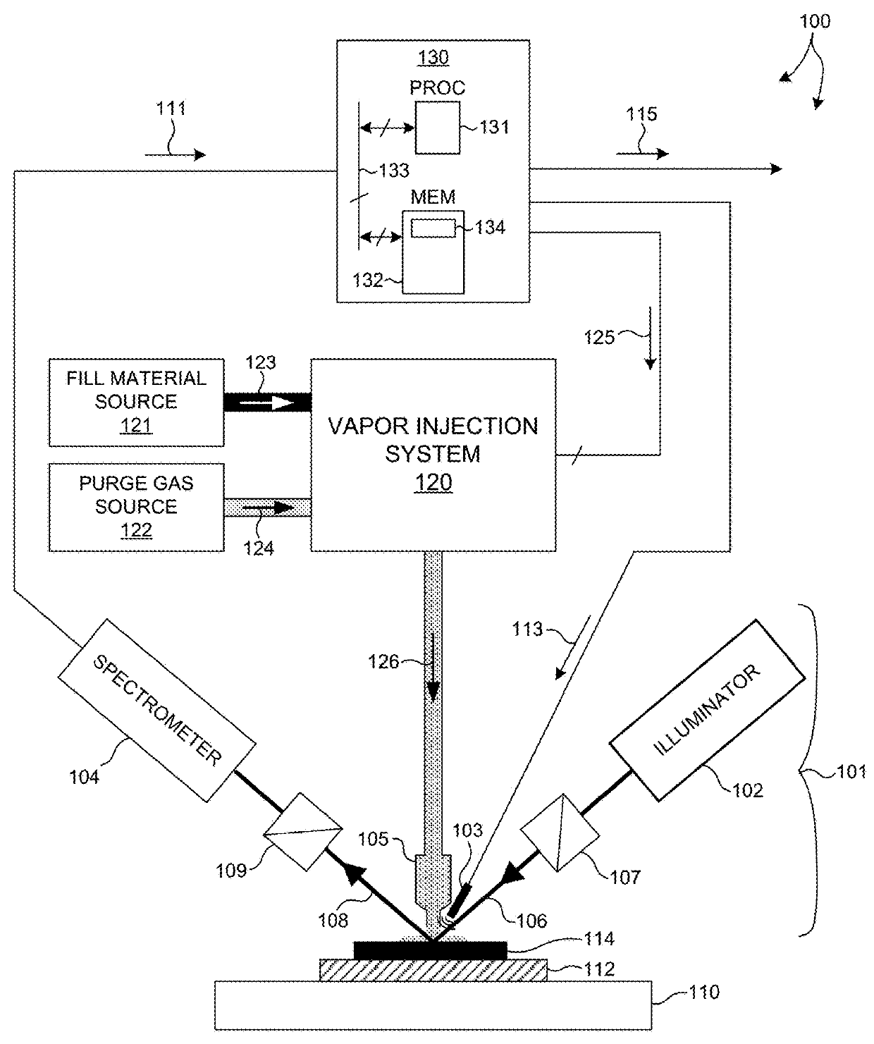
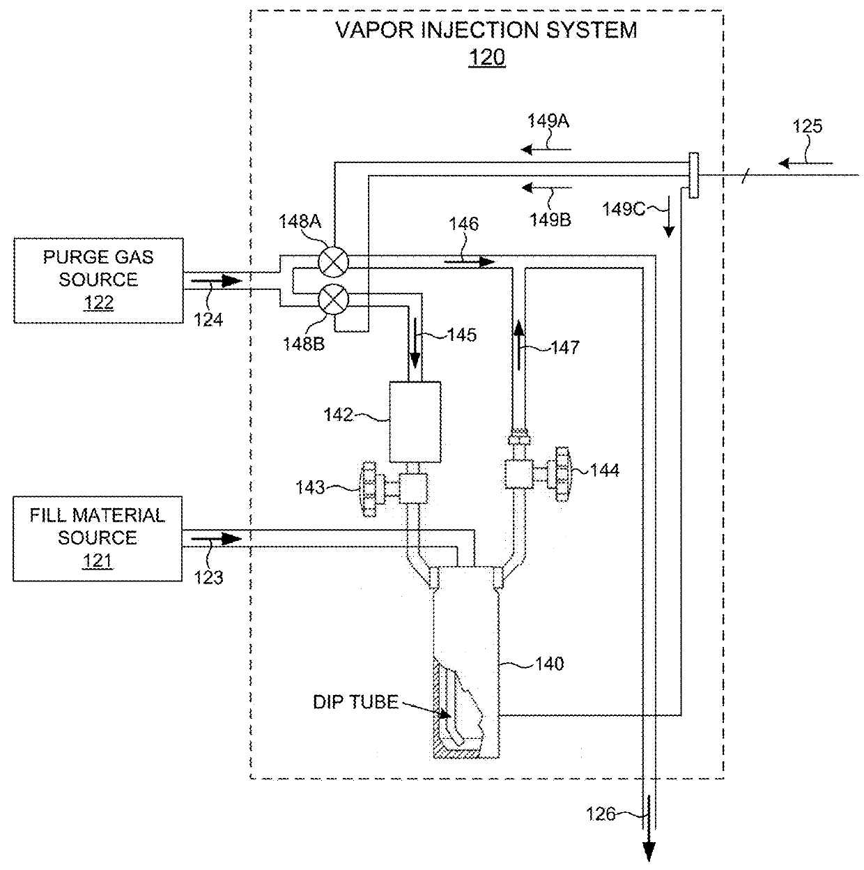
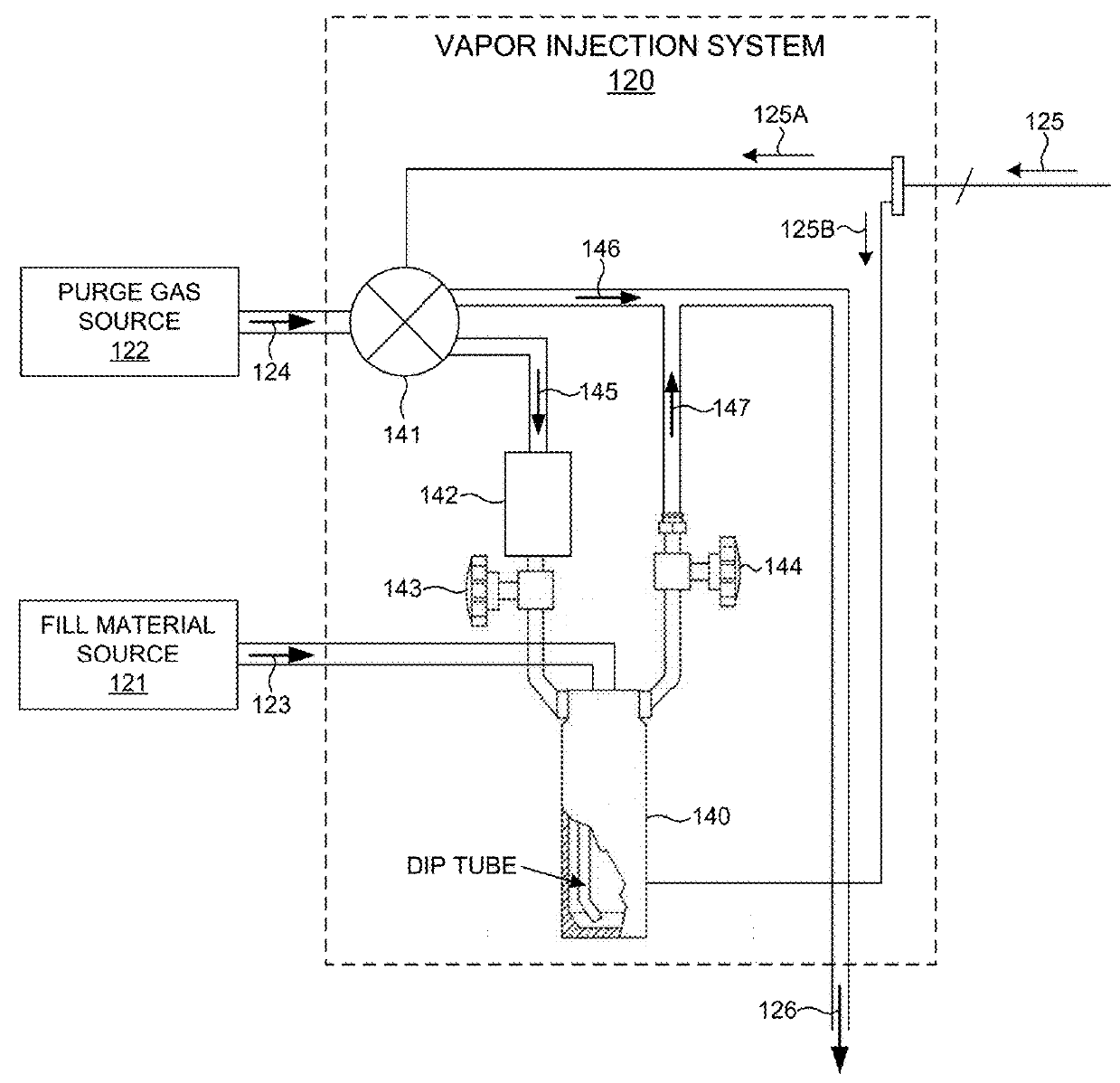
[0034]Reference will now be made in detail to background examples and some embodiments of the invention, examples of which are illustrated in the accompanying drawings.

[0035]Methods and systems for performing porosity measurements of semiconductor structures filled with a condensate by a capillary condensation process are presented herein. Optical measurements of porosity are performed while the local environment around the structures of interest are treated with a flow of purge gas that includes a controlled amount of fill material. A portion of the fill material (i.e., the condensate) condenses onto the structures under measurement and fills openings in the structural features, openings between structural features, etc. The presence of the condensate changes the optical properties of the structure under measurement compared to a measurement scenario where the purge gas is devoid of any fill material.

[0036]In some examples, multiple measurements of a structure are performed for dif...


PUM

PropertyMeasurementUnit
wavelength rangeaaaaaaaaaa
temperatureaaaaaaaaaa

Abstract

Methods and systems for performing optical measurements of the porosity of geometric structures filled with a fill material by a capillary condensation process are presented herein. Measurements are performed while the structure under measurement is treated with a flow of purge gas that includes a controlled amount of vaporized fill material. A portion of the fill material condenses and fills openings in the structural features such as pores of a planar film, spaces between structural features, small volumes such as notches, trenches, slits, contact holes, etc. In one aspect, the desired degree of saturation of vaporized material in the gaseous flow is determined based on the maximum feature size to be filled. In another aspect, measurement data is collected when a structure is unfilled and when the structure is filled. The collected data is combined in a multi-target model based measurement to estimate values of porosity and critical dimensions.

Description

CROSS REFERENCE TO RELATED APPLICATION[0001]The present application for patent claims priority under 35 U.S.C. § 119 from U.S. provisional patent application Ser. No. 62 / 330,751, entitled “Porosity and Critical Dimension Measurements Using Capillary condensation,” filed May 2, 2016, and from U.S. provisional patent application Ser. No. 62 / 441,887, entitled “Critical Dimension Measurements Using Liquid Filling,” filed Jan. 3, 2017, and from U.S. patent application Ser. No. 15 / 204,938, entitled “Critical Dimension Measurements With Capillary Condensation,” filed Jul. 7, 2016, the subject matter of each is incorporated herein by reference in its entirety.TECHNICAL FIELD[0002]The described embodiments relate to metrology systems and methods, and more particularly to methods and systems for improved measurement of structures fabricated in the semiconductor industry.BACKGROUND INFORMATION[0003]Semiconductor devices such as logic and memory devices are typically fabricated by a sequence of...

Claims


Application Information

Patent Timeline
Patent Type & Authority Patents(United States)
IPC IPC(8): G01N21/00G03F7/00G01B11/12G01N15/08
CPCG01N15/088G01B11/12G01N21/00G03F7/00G01N15/0806G01B2210/56G01N21/91G01N2021/213G01N2021/8427H01L22/12H01L22/24H01L22/30
Inventor KRISHNAN, SHANKAR
Owner KLA CORP
Why Eureka
Try Eureka