
Pyroelectric device

a pyroelectric device and pyroelectric technology, applied in the direction of thermoelectric devices with dielectric constant thermal change, semiconductor devices, electrical devices, etc., can solve the problems of limiting factors, reducing the overall efficiency and sensitivity of pyroelectric devices, and reducing the performance of typical thin-film pyroelectric devices, etc., to achieve increased overall efficiency and sensitivity of pyroelectric devices, and large net

Active Publication Date: 2018-08-07
ARMY US SEC THE
View PDF4 Cites 1 Cited by
  • Summary
  • Abstract
  • Description
  • Claims
  • Application Information

AI Technical Summary

Benefits of technology

The patent describes a new device that uses nanometer-sized pyroelectric elements that are insulated from each other and have a unique orientation relative to the electrodes, resulting in increased efficiency and sensitivity. The device can produce a large net pyroelectric response, even in response to small temperature changes. The device can also be enhanced by modifying the strain in the pyroelectric elements using a dielectric matrix material with a lower thermal expansion coefficient than the substrate material. This results in compressive strain around the pyroelectric elements, which can enhance the pyroelectric response. Overall, the device has higher sensitivity and fidelity than previously known pyroelectric devices.

Problems solved by technology

The pyroelectric properties are thus compromised and diminished by misaligned domains in these materials.
Therefore, typical thin-film pyroelectric devices will show reduced performance when integrated into common complimentary metal-oxide semiconductor (CMOS) processing.
This is a limiting factor when attempting to integrate pyroelectric devices directly into semiconductor fabrication, such as manufacturing pyroelectric arrays directly on silicon-based read-out circuitry.

Method used


Image

  • Pyroelectric device
  • Pyroelectric device
  • Pyroelectric device

Examples


example

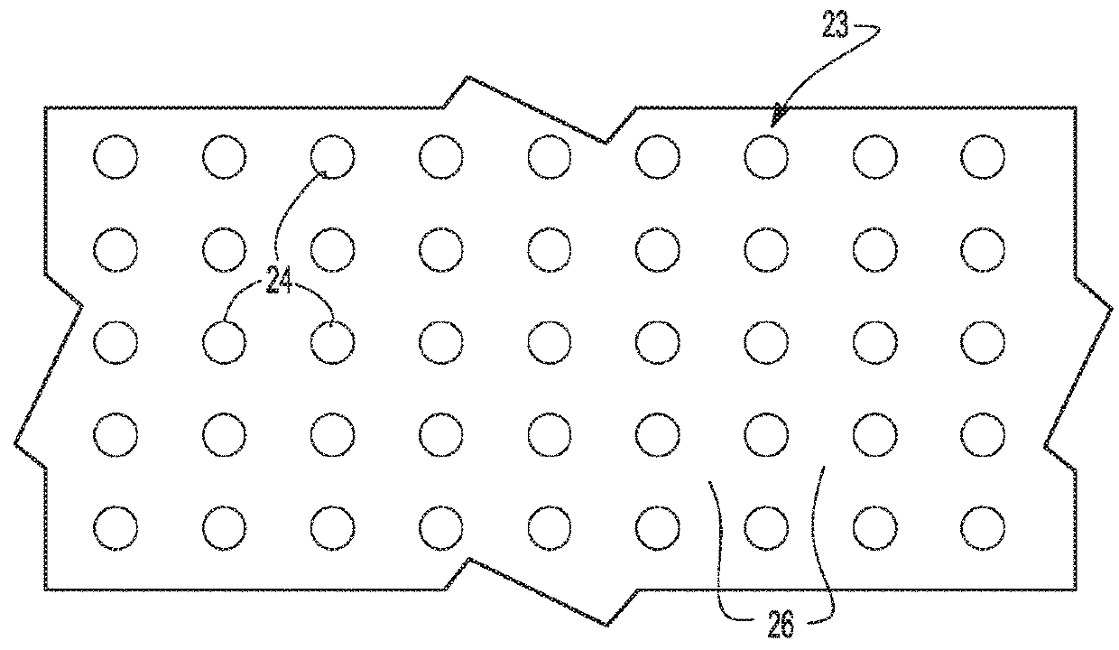
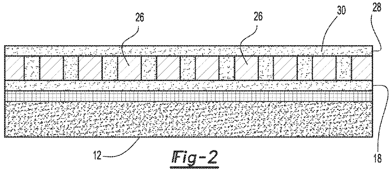
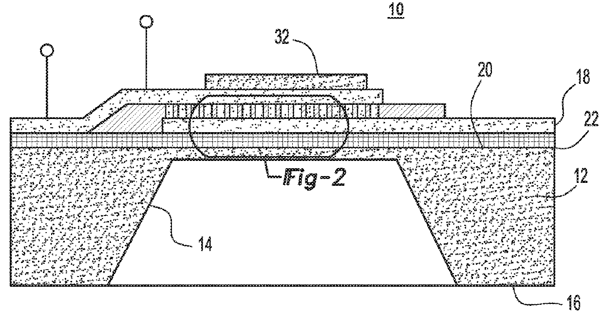
[0049]Certain preferred embodiments of the present invention have advantages over traditional thin-film pyroelectric materials. One preferred embodiment consists of pyroelectric nano-elements made from barium strontium titanate (BST), with composition Ba0.6Sr0.4TiO3, and a dielectric matrix of SiO2 fabricated on a sapphire substrate. Other examples of BST compositions and their derivatives include, but are not limited to, the BST compositions and / or structures described in U.S. Pat. Nos. 9,506,153, 8,216,701, 6,803,134 and 6,803,071 which are hereby incorporated by reference herein. Numerical simulations of the pyroelectric coefficient and detection figure of merit (FoM) are calculated using the phenomenological Landau-Devonshire theory and thermal strain in the film. Although we illustrate results for BST, the concept should be general to other ferroelectrics as well.

[0050]The most prominent source of strain for films on non-lattice matched substrates is the thermal strain created ...


PUM


Abstract

A pyroelectric device having a substrate and a first electrode overlying at least a portion of the substrate. A plurality of spaced apart nanometer sized pyroelectric elements are electrically connected to and extending outwardly from the first electrode so that each element forms a single domain. A dielectric material is deposited in the space between the individual elements and a second electrode spaced apart from said first electrode is electrically connected to said pyroelectric elements.

Description

CROSS-REFERENCE TO RELATED APPLICATIONS[0001]This application is a continuation-in-part of U.S. patent application Ser. No. 14 / 490,777 filed on Sep. 19, 2014 now U.S. Pat. No. 9,666,729 by inventors Ryan C. Toonen, Mathew P. Ivill and Melanie Will-Cole titled “Nano-Structured Paraelectric or Supra Electric Varactors for Agile Electronic Systems” which is hereby incorporated herein by reference in its entirety including all attachments, appendices and figures filed with U.S. Non-Provisional patent application Ser. No. 14 / 907,777.GOVERNMENT INTEREST[0002]The invention described herein may be manufactured, used, and licensed by or for the United States Government.BACKGROUND OF THE INVENTION[0003]I. Field of the Invention[0004]The present invention relates generally to pyroelectric devices.[0005]II. Description of Related Art[0006]Pyroelectricity, or the pyroelectric effect, is a physical property of polar dielectric materials which undergo a spontaneous change in polarization of the ma...

Claims


Application Information

Patent Timeline
Patent Type & Authority Patents(United States)
IPC IPC(8): H01L37/02H01L27/16H01L29/06B82Y10/00H01L29/66H01L29/93H10N15/10H10N19/00
CPCH01L37/025B82Y10/00H01L27/16H01L37/02H01L29/0676H01L29/66174H01L29/93H01L29/0653H10N19/00H10N15/15H10N15/10
Inventor TOONEN, RYAN C.IVILL, MATHEW P.COLE, MELANIE W.
Owner ARMY US SEC THE
Learn More