Light source device and projector

a light source device and projector technology, applied in the direction of semiconductor devices, light source devices, lighting and heating devices, etc., can solve the problems of increasing the thickness of the device, the problem of remarkable size, and the increase of the device planar size, so as to reduce the size of the projector

Active Publication Date: 2018-08-21
SEIKO EPSON CORP
View PDF9 Cites 0 Cited by
  • Summary
  • Abstract
  • Description
  • Claims
  • Application Information

AI Technical Summary

Benefits of technology

[0011]According to this configuration, the light source device includes the plurality of light emitting elements disposed on the base substrate, and the first polarity terminal and the second polarity terminal (input terminals). The input terminals project from one side of the base substrate as viewed in the third direction. With this configuration, it is possible to provide the light source device that emits high luminance light and is of small size.
[0012]Moreover, since it is sufficient that a drive circuit of the light source device is configured so as to be connected to the input terminals provided on one side of the base substrate, it is possible to reduce the size of the drive circuit and thus to reduce the size of an apparatus on which this light source device is mounted. Thus, it is possible to provide the light source device that can contribute to reducing the size of the apparatus. In particular, a remarkable advantageous effect is provided for an apparatus on which a plurality of light source devices are mounted.Application Example 2
[0018]According to this configuration, it is possible to provide the light source device that efficiently emits light to the side opposite to the base substrate.
[0019]Moreover, the holding portion and the light emitting element group held by the holding portion can be configured as a sub-unit in which the holding portion and the light emitting element group are integrated together. Therefore, compared to a configuration in which the light emitting elements are individually disposed on the base substrate, it is possible to manufacture the light source device in which a variation in optical characteristics of the plurality of light emitting elements is reduced, or the light source device can be repaired by exchanging the sub-unit in the case of the occurrence of a failed light emitting element. Thus, it is possible to provide the light source device that efficiently emits light to the side opposite to the base substrate, has less variation in optical characteristics, and can be easily repaired.Application Example 5
[0021]According to this configuration, since the light source device includes the auxiliary substrate, it is possible to improve the flexibility of the connection path between each of the light emitting element groups and the second polarity terminal.
[0030]According to this configuration, since the projector includes the light source device described above, it is possible to project a bright image while reducing the size of the projector.

Problems solved by technology

However, the technique disclosed in JP-A-2014-116227 has a problem in that the thickness of the device is increased because of the configuration in which the lead wires are inserted through the substrate of the light source device.
Therefore, when the light source device disclosed in JP-A-2014-116227 is configured using the configuration of the terminals disclosed in JP-A-2006-114661, there arises a problem in that the planar size of the device is increased.
In particular, when an apparatus including a plurality of light source devices is configured, the problem becomes remarkable.

Method used


Image

  • Light source device and projector
  • Light source device and projector
  • Light source device and projector

Examples


first embodiment

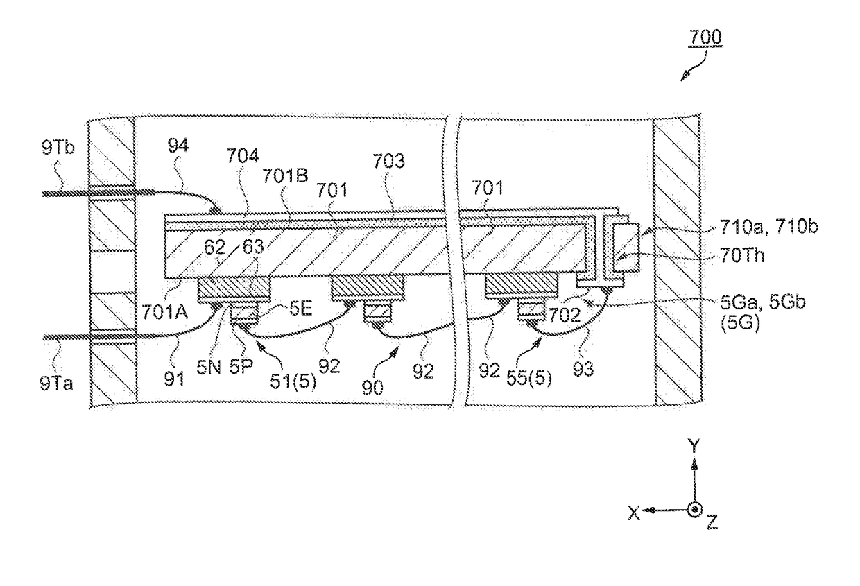
[0048]Hereinafter, a light source device and a projector according to a first embodiment will be described with reference to the drawings. In the drawings shown below, dimensions and ratios of components are appropriately different from actual ones in order to show the components in sizes recognizable on the drawings.

Main Configuration of Projector

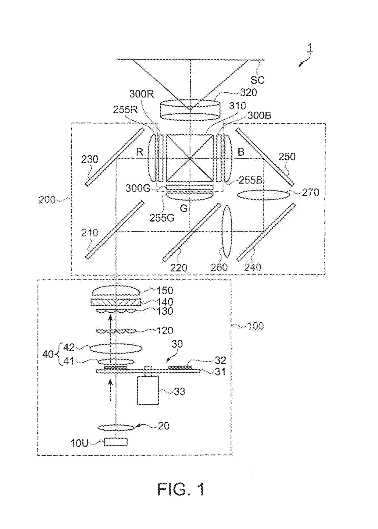
[0049]FIG. 1 is a schematic view showing an optical system of a projector 1 according to the embodiment.

[0050]As shown in FIG. 1, the optical system of the projector 1 includes an illumination device 100, a color separation optical system 200, light modulators 300R, 300G, and 300B, a cross dichroic prism 310 as a color combining optical device, and a projection optical device 320. Although not shown in the drawing, the projector 1 includes, in addition to the optical system described above, a control section that controls the operation of the projector 1, a power source device that supplies power to the illumination device 100 and the cont...

second embodiment

[0118]Hereinafter, a light source device 400 according to a second embodiment will be described with reference to the drawing. In the following description, components similar to those of the first embodiment are denoted by the same reference numerals and signs, and the detailed description of the components is omitted or simplified.

[0119]The light source device 400 of the embodiment includes wiring different from the wiring of the light source device 10 of the first embodiment.

[0120]FIG. 10 is a schematic view for explaining the wiring of the light source device 400.

[0121]Similarly to the light source device 10 of the first embodiment, the light source device 400 of the embodiment includes the four light emitting element groups 5Ga, 5Gb, 5Gc, and 5Gd, and one row of the light emitting elements 5 in each of the light emitting element groups 5G are connected in series.

[0122]The light source device 400 includes a second conductive layer 164 having patterns different from the pattern o...

third embodiment

[0131]Hereinafter, a light source device 600 according to a third embodiment will be described with reference to the drawings. In the following description, components similar to those of the light source devices 10 and 400 described above are denoted by the same reference numerals and signs, and the detailed description of the components is omitted or simplified.

[0132]The light source device 600 of the embodiment includes an auxiliary substrate 610 in addition to the components of the light source devices 10 and 400, and similarly to the light source device 400, the second polarity terminal 9Tb is connected in common to the light emitting element groups 5G. Moreover, the light source device 600 includes a base substrate 16 different from the base substrate 6 described above.

[0133]FIG. 11 is a cross-sectional view schematically showing the light source device 600. FIG. 12 is a plan view schematically showing the light source device 600.

[0134]As shown in FIGS. 11 and 12, the base sub...


PUM


Abstract

A light source device includes: a base substrate; a plurality of light emitting elements disposed on the base substrate along each of an X-direction and a Y-direction crossing the X-direction; and a first polarity terminal and a second polarity terminal for supplying power to the plurality of light emitting elements. The first polarity terminal and the second polarity terminal project from one side of the base substrate in the X-direction as viewed in a Z-direction orthogonal to the X-direction and the Y-direction.

Description

CROSS REFERENCE TO RELATED APPLICATION[0001]The entire disclosure of Japanese Patent Application No. 2016-098480, filed on May 17, 2016 and Japanese Patent Application No. 2017-048367, filed on Mar. 14, 2017 is expressly incorporated by reference herein.BACKGROUND1. Technical Field[0002]The present invention relates to a light source device and a projector.2. Related Art[0003]A light source for illumination including a plurality of light emitting elements has been known in the related art (e.g., see JP-A-2014-116227). Moreover, a technique of enclosing a light receiving element and a light source such as a semiconductor laser in a package has been proposed (e.g., see JP-A-2006-114661).[0004]The light source for illumination disclosed in JP-A-2014-116227 includes a t source device (light emitting diode (LED) module), lead wires, and a lighting circuit.[0005]The LED module includes a substrate and a plurality of LEDs (light emitting elements) disposed on the substrate. The plurality o...

Claims


Application Information

Patent Timeline
Patent Type & Authority Patents(United States)
IPC IPC(8): G03B21/20H01L25/075F21V23/06F21V23/00H01L33/62F21Y105/10F21Y115/30
CPCG03B21/2013F21V23/001F21V23/06G03B21/204H01L25/0753H01L33/62F21Y2105/10H01L2924/19107F21Y2115/30H01L2224/48091H01L2924/16195H01L2924/00014G03B21/20G03B21/2033
Inventor TAKAGI, CHIGUSA
Owner SEIKO EPSON CORP
Why Eureka
Try Eureka