Substrate packaging structure and packaging method thereof

a packaging structure and substrate technology, applied in the direction of solid-state devices, manufacturing tools, laser beam welding apparatus, etc., can solve the problems of reducing the quality of the package, voids or cracks in the frit, etc., and achieve the effect of reducing the thermal defect of the fri

Active Publication Date: 2018-08-28
AU OPTRONICS CORP
View PDF12 Cites 0 Cited by
  • Summary
  • Abstract
  • Description
  • Claims
  • Application Information

AI Technical Summary

Benefits of technology

[0008]This invention provides a substrate packaging structure with a light-diffusing component, in order to decrease the thermal defect of the frit.
[0019]Another aspect of this invention is providing a packaging method for said substrate packaging structure. The packaging method includes the steps of: providing an upper substrate and a lower substrate and the top surface of the upper substrate having a light-diffusing component; disposing a frit between the upper substrate and the lower substrate; and providing a laser beam to irradiate the substrate packaging structure. The frit is irradiated by the laser beam through the light-diffusing component so that the irradiating area is increased.
[0021]In the packaging method, because of the light-diffusing component disposed on the upper substrate, the laser beam is diffused by the light-diffusing component so that the irradiation angle thereof is increased. Thus, the irradiation area of the laser beam and the heating time of the frit are increased. The front part of the laser beam pre-heats the frit, the central part of the laser beam melts the frit and the back part of the laser beam prevents the frit from cooled too fast. Because the heating and cooling speed of the frit is slowed down during the packaging process, the thermal defects such as voids and cracks may be avoided effectively. Because the light-diffusing component is disposed on the upper substrate, the related equipment of the laser beam needs not be amended or modified so that the cost is saved.

Problems solved by technology

However, during sintering the frit, owing to the thermal shock (rapid heating and cooling), the thermal defects, for example, voids or cracks are produced in the frit.
Thus, the quality of the seal is affected so that the quality of the package is reduced.

Method used


Image

  • Substrate packaging structure and packaging method thereof
  • Substrate packaging structure and packaging method thereof
  • Substrate packaging structure and packaging method thereof

Examples


Embodiment Construction

[0030]Reference will now be made in detail to the present embodiments of the invention, examples of which are illustrated in the accompanying drawings. Wherever possible, the same reference numbers are used in the drawings and the description to refer to the same or like parts.

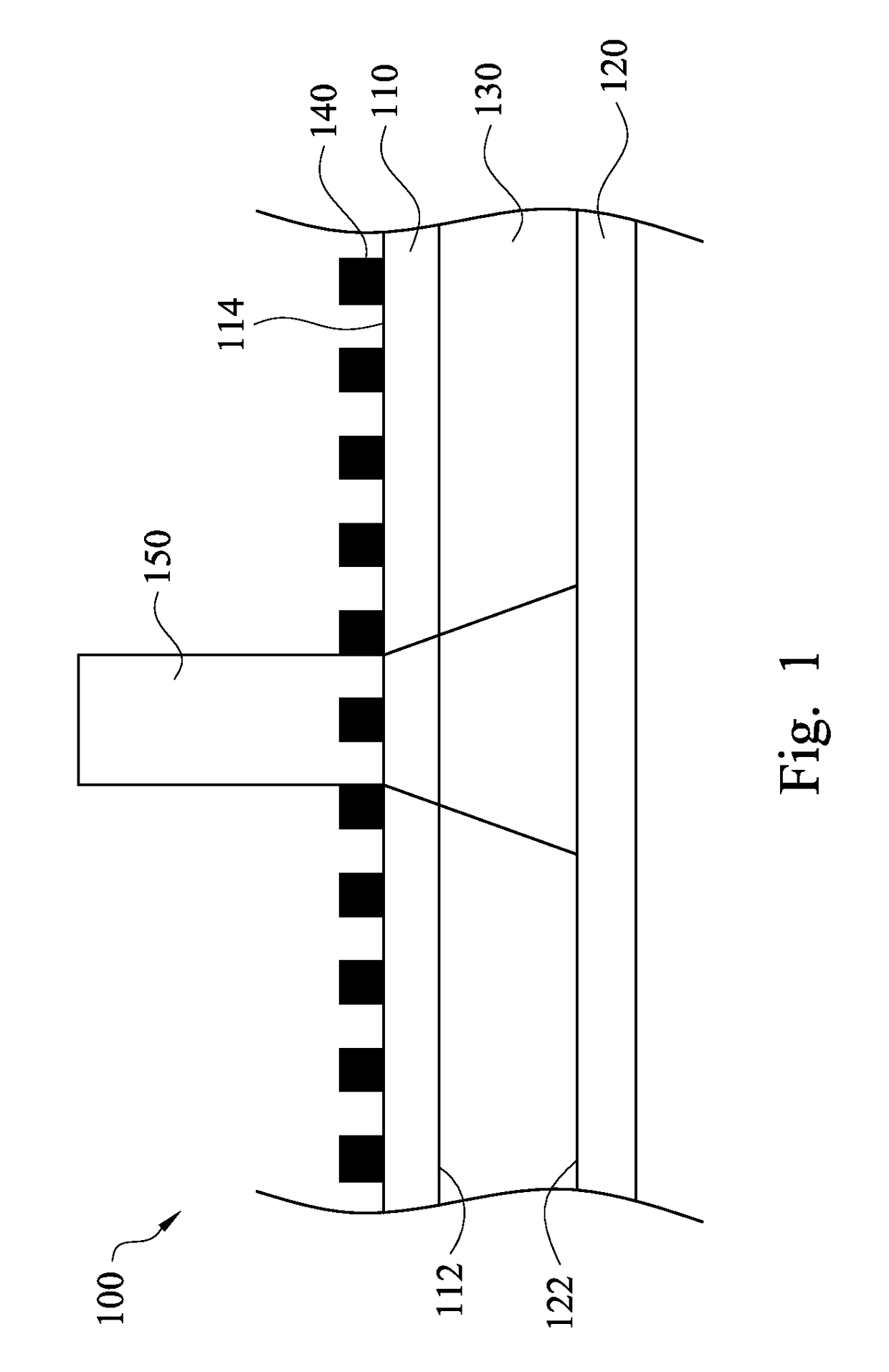
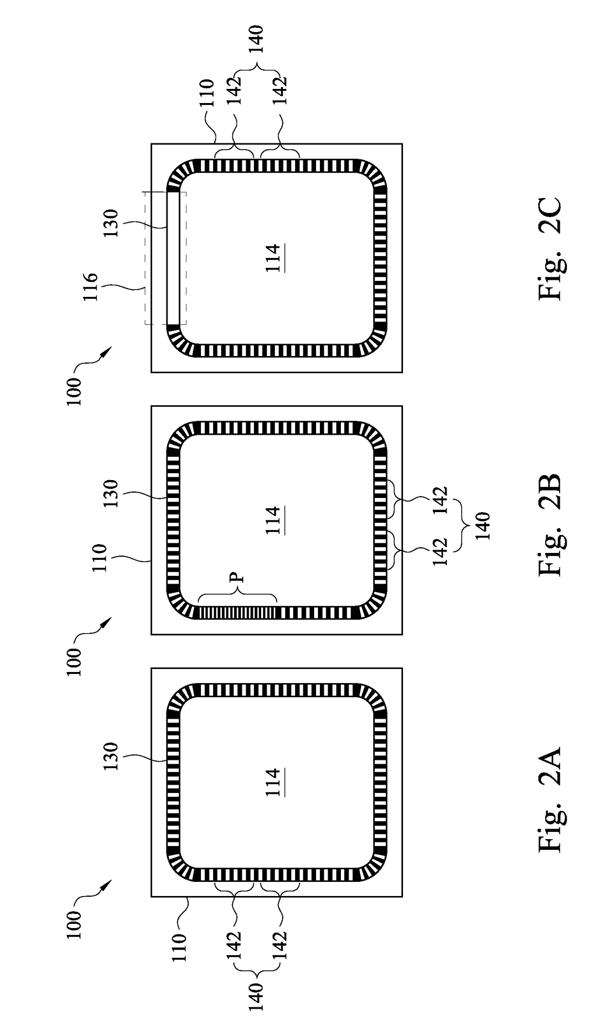
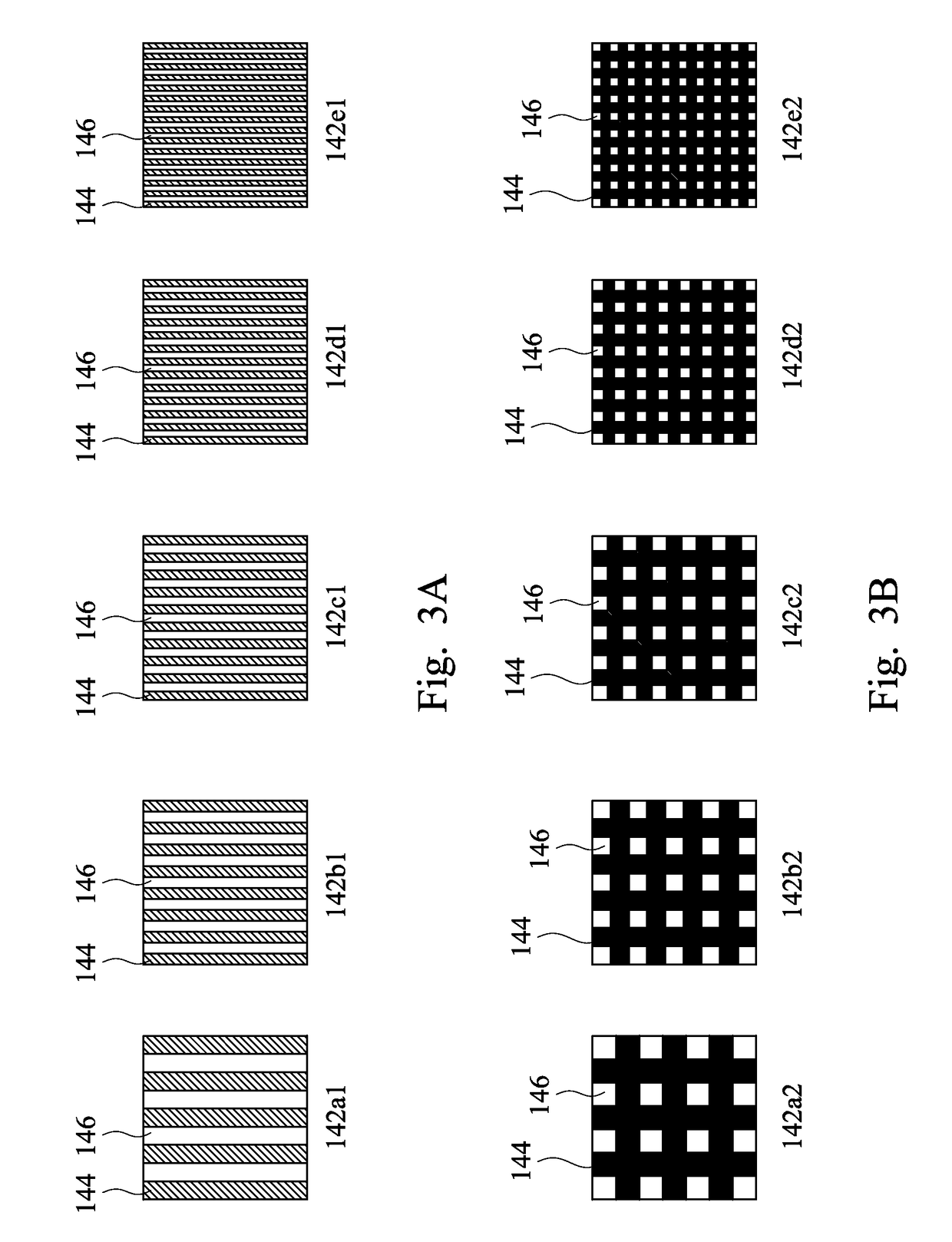
[0031]Referring to FIG. 1, FIG. 1 is a schematic cross-section view of the substrate packaging structure according to one embodiment of this invention. The substrate packaging structure 100 includes an upper substrate 110, a lower substrate 120, a frit 130, and a light-diffusing component 140. The frit 130 is disposed between the upper substrate 110 and the lower substrate 120. The light-diffusing component 140 is disposed on the upper substrate 110.

[0032]The frit 130 is disposed between the upper substrate 110 and the lower substrate 120. Further, the frit 130 is distributed between the upper substrate 110 and the lower substrate 120 and substantially in a frame shape. The frit 130 is a thermoplastic colloid,...


PUM

PropertyMeasurementUnit
widthaaaaaaaaaa
widthaaaaaaaaaa
widthaaaaaaaaaa

Abstract

A substrate packaging structure includes an upper substrate, a lower substrate, a frit disposed there between for adhering the upper substrate and the lower substrate, and a light-diffusing component. The light-diffusing component is disposed on the upper substrate and corresponding to the frit. The light-diffusing component is utilized for diffusing a laser beam.

Description

RELATED APPLICATIONS[0001]This application claims priority to Taiwan Application Serial Number 103101829, filed Jan. 17, 2014, which is herein incorporated by reference.BACKGROUND[0002]Field of Invention[0003]The present invention relates to a substrate packaging structure.[0004]Description of Related Art[0005]Nowadays, the technology of the touch display is developed vigorously. Generally, the touch display panel module is composed of a touch panel and a display module. Generally, during the process of the package, in order to improve the seal between two glass substrates, the frit is utilized as the medium to adhere the glass substrates. Then, the laser beam heats and sinters the frit to adhere two glass substrates so that two glass substrates are sealed to avoid the effect of the moisture and oxygen from the environment.[0006]In order to improve the efficiency of the package process, the time of the laser heating is short, so the heating temperature should be high enough to provi...

Claims


Application Information

Patent Timeline
Patent Type & Authority Patents(United States)
IPC IPC(8): B23K26/00B23K26/06B23K26/064B23K26/20H01L51/52
CPCB23K26/064B23K26/009B23K26/206B23K26/0661H01L51/524H10K50/841
Inventor HSIAO, CHIH-HUNGCHANG, WEI-CHIHWENG, CHOU-CHIN
Owner AU OPTRONICS CORP
Why Eureka
Try Eureka