Circuit substrate, and noise reduction method for circuit substrate

a circuit substrate and noise reduction technology, applied in the field of circuit substrates, can solve problems such as signal degradation, and achieve the effect of reducing the gap structure of the electromagnetic band and effectively using mounting spa

Active Publication Date: 2018-10-23
YAMAHA CORP
View PDF13 Cites 0 Cited by
  • Summary
  • Abstract
  • Description
  • Claims
  • Application Information

AI Technical Summary

Benefits of technology

[0017]As described above, the present invention performs capacitance loading to a first electromagnetic band gap structure by using an auxiliary pattern, and decreases a resonance frequency of the first electromagnetic band gap structure. Accordingly, according to the present invention, the first electromagnetic band gap structure can be minimized and the mounting space can be effectively used, compared to a case where the resonance frequency is decreased by increasing a length of an outer circumference of the first electromagnetic band gap structure in the same manner as in the related art.

Problems solved by technology

Accordingly, there is a problem in which electromagnetic noise that is generated by an operation clock of a central processing unit (CPU), a memory, or the like in the digital circuit, interferes with the analog circuit, and thus the signal for communication is degraded.

Method used


Image

  • Circuit substrate, and noise reduction method for circuit substrate
  • Circuit substrate, and noise reduction method for circuit substrate
  • Circuit substrate, and noise reduction method for circuit substrate

Examples


Embodiment Construction

[0027]Hereinafter, an embodiment of the present invention will be described with reference to the drawings.

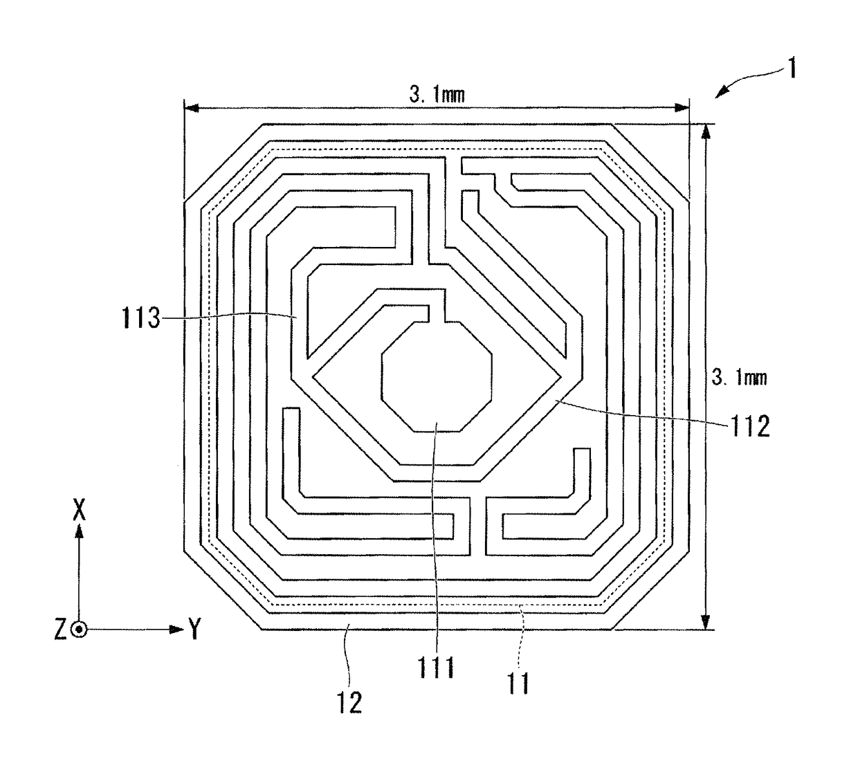
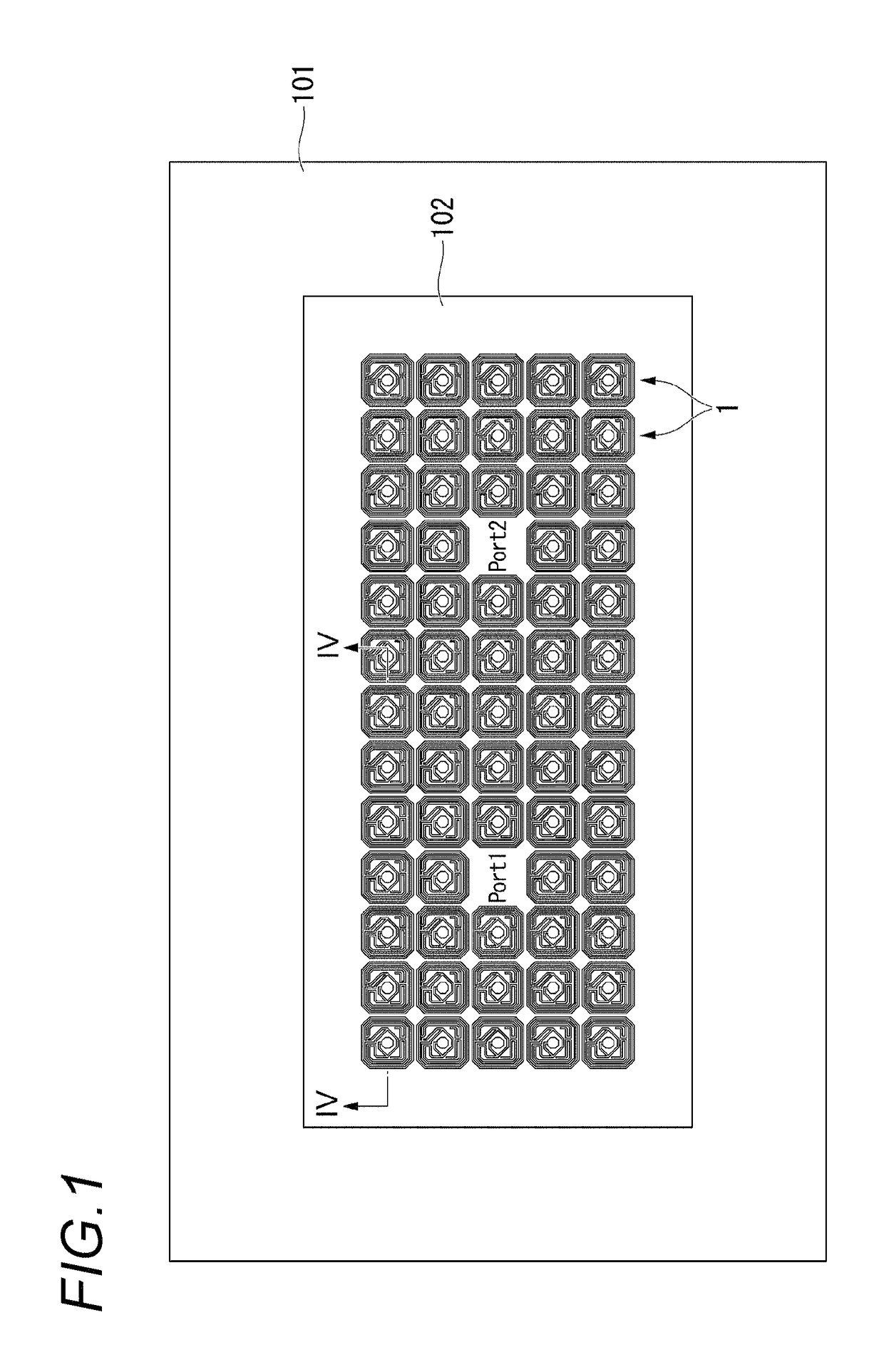
[0028]FIG. 1 is a plan view illustrating an example of a printed circuit substrate according to an embodiment of the present invention. FIG. 1 is a view in which a configuration of FIG. 9 that is a conceptual diagram of a basic configuration of an artificial magnetic conductor according to the present invention which will be described below is more specified in correspondence with the embodiment which will be described below. A power plane 102 is provided in an overlapping manner on an upper portion of one main surface (front surface) of a reference plane (for example, ground plane) 101. The power plane 102 is provided such that the other main surface (rear surface) thereof faces an upper surface (front surface) of the reference plane 101. The power plane 102 is provided such that the electromagnetic band gap structural bodies 1 are arranged in a predetermined cycle and in a ma...


PUM


Abstract

A circuit substrate includes a core substrate, a reinforcing dielectric layer that is provided on one surface of the core substrate, a first electromagnetic band gap structure that is provided on one surface side of the reinforcing dielectric layer and reduces electromagnetic noise in a predetermined first frequency propagating through the core substrate, and an auxiliary pattern that is formed at a predetermined distance from an outer circumference of a pattern which forms the first electromagnetic band gap structure.

Description

TECHNICAL FIELD[0001]The present invention relates to a circuit substrate in which electronic components are mounted and a noise reduction method for the circuit substrate.BACKGROUND ART[0002]According to demand for miniaturization of electronic components, a large quantity of integrated circuit chips or circuit components are required to be mounted on an electronic circuit substrate on which a semiconductor integrated circuit or the circuit components are mounted. Accordingly, demand for effective use of a wiring space or a mounting space is increasing.[0003]Particularly, a signal which is used for information processing of an electronic circuit is a digital signal in a wireless local area network (LAN) communication, and thus an analog circuit which performs wireless communication and a digital circuit which performs information processing of a signal for communication are used together.[0004]Accordingly, there is a problem in which electromagnetic noise that is generated by an op...

Claims


Application Information

Patent Timeline
Patent Type & Authority Patents(United States)
IPC IPC(8): H04B3/28H05K1/02
CPCH05K1/025H05K1/0236H05K1/0298H05K1/16
Inventor KAWATA, AKIHIRO
Owner YAMAHA CORP
Why Eureka
Try Eureka