
Nanosheet CMOS transistors

a technology of nanosheets and transistors, applied in the direction of basic electric elements, semiconductor devices, electrical equipment, etc., can solve the problems of poor device performance, topography problems, and channel structure that can significantly influence the electrical properties of the devi

Active Publication Date: 2019-04-16
INT BUSINESS MASCH CORP
View PDF12 Cites 5 Cited by
  • Summary
  • Abstract
  • Description
  • Claims
  • Application Information

AI Technical Summary

Benefits of technology

This approach results in higher-quality silicon germanium channels that are co-planar with silicon channels, enhancing device performance and addressing topography issues, thereby improving the fabrication of nanosheet channel transistors.

Problems solved by technology

The geometry of the channel structure can significantly impact the electrical properties of the device.
However, current nanosheet fabrication processes use epitaxial processes that result in relatively low-quality nanosheet structures, resulting in poor device performance.
This will introduce topography issues in the downstream device fabrication processes since the channels in the respective regions would be offset relative to each other and thus would not be at the same level in the final device.

Method used


Image

  • Nanosheet CMOS transistors
  • Nanosheet CMOS transistors
  • Nanosheet CMOS transistors

Examples


Embodiment Construction

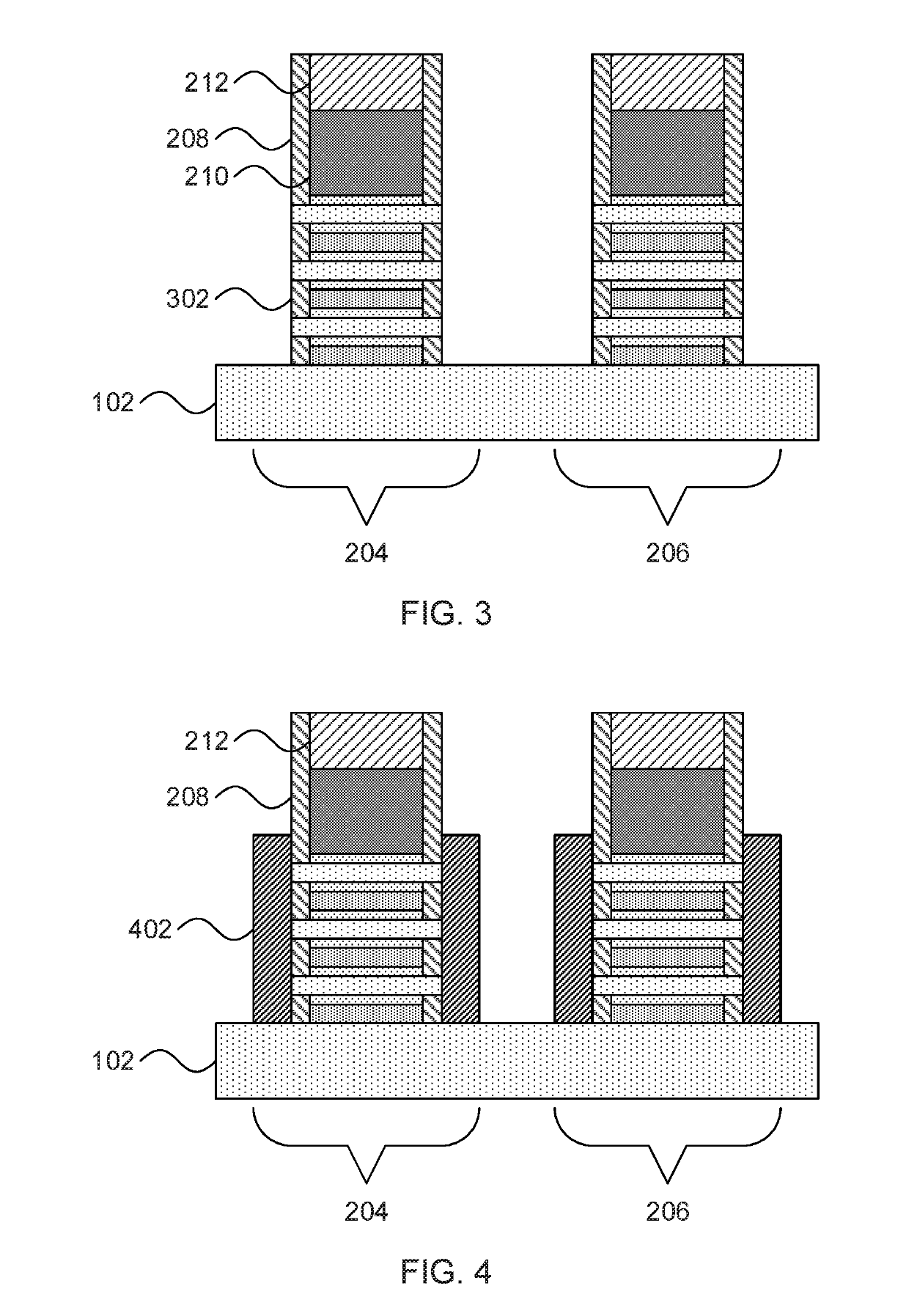
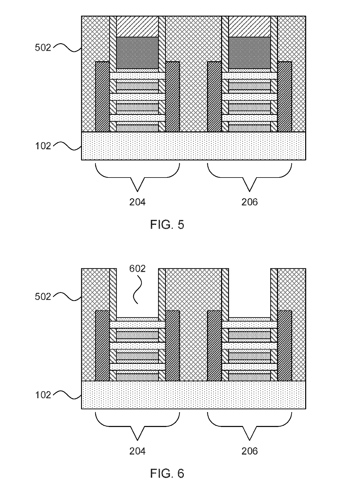
[0021]Embodiments of the present invention provide silicon and silicon germanium nanosheet channel transistors on a single chip. Rather than growing the silicon germanium nanosheet structures epitaxially, existing silicon nanosheets are annealed to convert those structures into silicon germanium nanosheets. The resulting silicon germanium channels are formed with a higher quality than epitaxially grown structures would be and are co-planar with the silicon channel structures that are formed on the same chip.

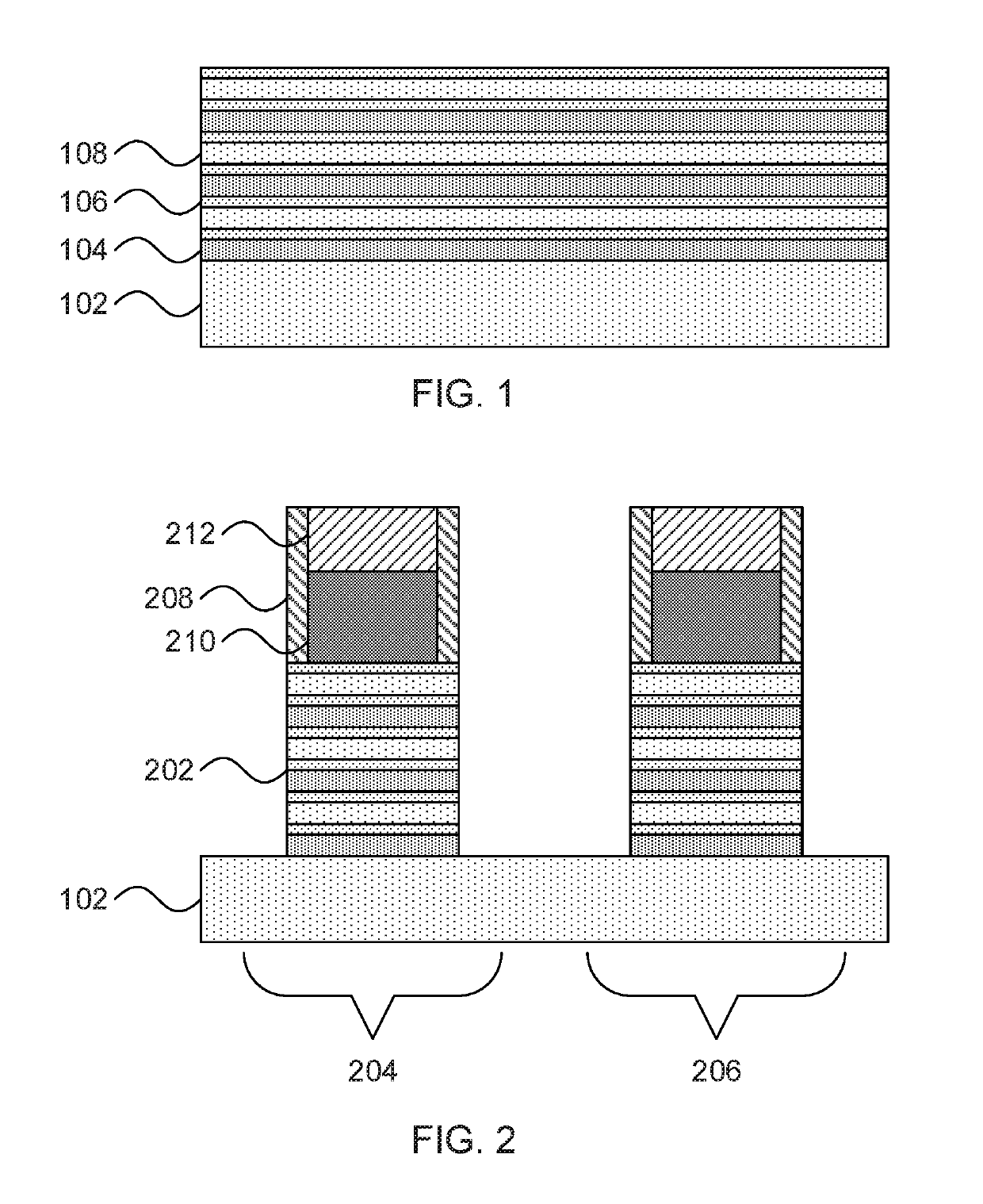
[0022]Referring now to FIG. 1, a cross-sectional view of a step in the fabrication of a nanosheet field effect transistor (FET) is shown. A stack of semiconductor layers is formed on a semiconductor substrate 102. The semiconductor substrate 102 may be a bulk-semiconductor substrate. In one example, the bulk-semiconductor substrate may be a silicon-containing material. Illustrative examples of silicon-containing materials suitable for the bulk-semiconductor substrate include, but...


PUM


Abstract

Methods of forming integrated chips include forming a respective stack of sheets in two regions, each stack having first layers and second layers. The second layers are etched away in the first region. The second region is annealed to change the composition of the first layers in the second region by interaction with the second layers in the second region. A gate stack is formed in the first and second region.

Description

BACKGROUND[0001]Technical Field[0002]The present invention generally relates to semiconductor device fabrication and, more particularly, to the formation of transistors having nanosheet channels.[0003]Description of the Related Art[0004]Field effect transistors (FETs) are semiconductor devices that use an electric field generated by a gate structure to influence the behavior of charge carriers within a semiconductor channel structure. The geometry of the channel structure can significantly impact the electrical properties of the device. N-type field effect transistors (NFET) and p-type field effect transistors (PFET) are two types of complementary metal oxide semiconductor FETs (MOSFETs). The NFET uses electrons as the current carriers and with n-doped source and drain junctions. The PFET uses holes as the current carriers and with p-doped source and drain junctions.[0005]Nanosheet channel structures present one option for scaling device architectures to smaller sizes. Nanosheet (or...

Claims


Application Information

Patent Timeline
Patent Type & Authority Patents(United States)
IPC IPC(8): H01L21/324H01L25/00H01L25/07H01L29/06H01L29/08H01L21/28
CPCH01L29/0684H01L21/28255H01L29/0843H01L25/07H01L25/50H01L21/324H01L25/072
Inventor BI, ZHENXINGCHENG, KANGGUOLI, JUNTAOXU, PENG
Owner INT BUSINESS MASCH CORP
Learn More