
Imaging device, image processing device, image processing method, program, and recording medium

a technology of image processing and imaging device, which is applied in the direction of image enhancement, closed-circuit television system, instruments, etc., can solve the problems of reducing the amount of peripheral light of wide-angle lenses, limiting the size and cost of optical systems that can be used in imaging devices, and reducing the quality of target images. , to achieve the effect of improving the quality of target images

Active Publication Date: 2019-04-23
FUJIFILM CORP
View PDF10 Cites 0 Cited by
  • Summary
  • Abstract
  • Description
  • Claims
  • Application Information

AI Technical Summary

Benefits of technology

The patent is about an image processing device that uses an optical system to capture images. The device includes a restoration processing unit that uses the optical transfer function to improve the image quality. The device can improve the MTF (Matrix Transformation Function) of the image by about 10% or more. The device can be used with different optical systems and can be integrated into or interchanged with those optical systems. The device can determine whether the MTF is reduced and perform the restoration process based on the information of the optical system. This is important because reducing the MTF by restoration can negligibly affect the overall image quality. The device can improve the image quality of the target image and increase the low SN ratio of the imaging element.

Problems solved by technology

The size and cost of an optical system that can be used in an imaging device are limited according to a usage environment or the user's needs.
However, in practice, an optical system that does not have a high resolution performance is generally used due to the above-mentioned limitations.
In particular, a wide-angle lens is likely to reduce the amount of peripheral light.
In a case in which a reduction in the amount of peripheral light is prevented under the limit of, for example, size and costs, it is difficult to sufficiently prevent the influence of aberration, which results in a reduction in the resolution of the captured image.
As such, it is difficult to manufacture a small, inexpensive, and high-performance optical system that can capture a wide-angle image.
In particular, since a trade-off relationship is established between the amount of peripheral light and aberration, it is very difficult to manufacture a small and inexpensive optical system which is used to capture a wide-angle image and has a high resolution performance while ensuring a sufficient amount of peripheral light.

Method used

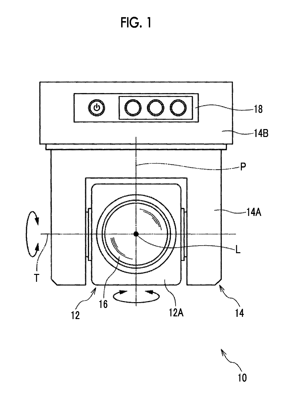
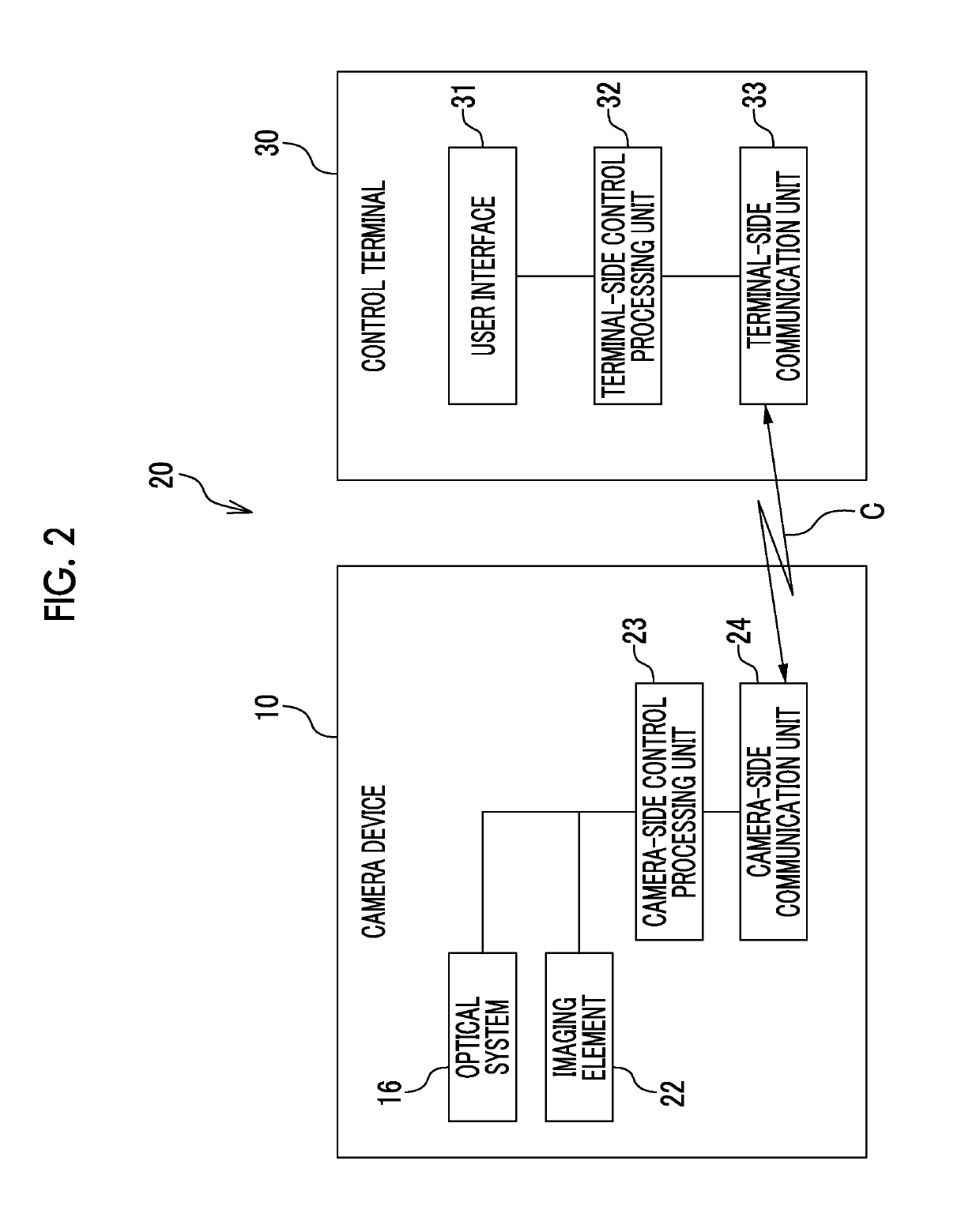
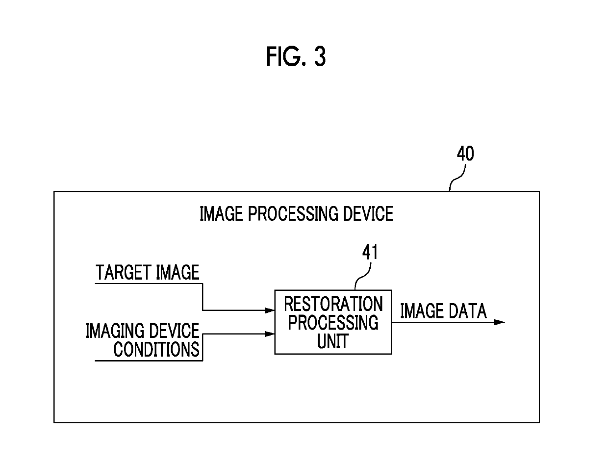

Image

  • Imaging device, image processing device, image processing method, program, and recording medium
  • Imaging device, image processing device, image processing method, program, and recording medium
  • Imaging device, image processing device, image processing method, program, and recording medium

Examples


example 1

[0243]FIG. 12 is a cross-sectional view illustrating an optical system 16 according to Example 1. The left side of FIG. 12 is an object side (subject side) and the right side thereof is an image side (the side of an image surface Sim).

[0244]The optical system 16 according to this example includes “a first optical element L1, a second optical element L2, a third optical element L3, a fourth optical element L4, and a fifth optical element L5”, a “stop St”, and “a sixth optical element L6, a seventh optical element L7, an eighth optical element L8, a ninth optical element L9, and a tenth optical element L10” which are arranged in this order from the object side.

[0245]In the optical system 16 according to this example, the stop St is fixed between “the first optical element L1, the second optical element L2, the third optical element L3, the fourth optical element L4, and the fifth optical element L5” and “the sixth optical element L6, the seventh optical element L7, the eighth optical ...

example 2

[0259]In this example, the same elements as those in Example 1 are denoted by the same reference numerals and the detailed description thereof will not be repeated.

[0260]FIG. 19 is a cross-sectional view illustrating an optical system 16 according to Example 2.

[0261]The optical system 16 according to this example includes “a first optical element L1, a second optical element L2, a third optical element L3, a fourth optical element L4, a fifth optical element L5, a sixth optical element L6, a seventh optical element L7, and an eighth optical element L8”, a “stop St”, and “a ninth optical element L9, a tenth optical element L10, an eleventh optical element L11, a twelfth optical element L12, a thirteenth optical element L13, and a fourteenth optical element L14” which are arranged in this order from the object side.

[0262]FIG. 20 is a table (Table 6) illustrating the basic data of the optical system 16 according to Example 2. FIG. 20 illustrates a “surface number R”, a “curvature radiu...

example 3

[0277]In this example, the same elements as those in Example 1 are denoted by the same reference numerals and the detailed description thereof will not be repeated.

[0278]FIG. 27 is a cross-sectional view illustrating an optical system 16 according to Example 3.

[0279]The optical system 16 according to this example includes “a first optical element L1, a second optical element L2, a third optical element L3, a fourth optical element L4, a fifth optical element L5, and a sixth optical element L6”, a “stop St”, and “a seventh optical element L7, an eighth optical element L8, a ninth optical element L9, a tenth optical element L10, an eleventh optical element L11, and a twelfth optical element L12” which are arranged in this order from the object side.

[0280]FIG. 28 is a table (Table 12) illustrating the basic data of the optical system 16 according to Example 3. FIG. 28 illustrates a “surface number R”, a “curvature radius r” (mm), a “surface interval d” (mm), an “effective radius er” (m...


PUM


Abstract

A restoration processing unit performs a restoration process based on an optical transfer function of an optical system for a target image. The entire angle of view of the optical system is greater than 90 degrees. A light amount evaluation region of the optical system is a region in which a distance from the center of an image formation plane is not less than 80% of half of the length of a diagonal line of an imaging surface of an imaging element. When a first evaluation wavelength is used, the ratio of the amount of light in the light amount evaluation region to the amount of light in a region of the optical system corresponding to the center of the image formation plane is not less than 25%. When a second evaluation wavelength is used, the value of the MTF of the optical system acquired at half of the Nyquist frequency of the imaging element is not less than 15%.

Description

CROSS-REFERENCE TO RELATED APPLICATIONS[0001]The present application is a Continuation of PCT International Application No. PCT / JP2016 / 061512 filed on Apr. 8, 2016 claiming priority under 35 U.S.C § 119(a) to Japanese Patent Application No. 2015-084393 filed on Apr. 16, 2015. Each of the above applications is hereby expressly incorporated by reference, in their entirety, into the present application.BACKGROUND OF THE INVENTION1. Field of the Invention[0002]The present invention relates to an imaging device, an image processing device, an image processing method, a program, and a recording medium, and more particularly, to a technique for restoring a captured wide-angle image.2. Description of the Related Art[0003]A captured image obtained by an imaging device, such as a digital camera, includes a degradation component such as blurring or distortion caused by, for example, the aberration of an optical system. It is preferable to perform imaging, using an optical system with small abe...

Claims


Application Information

Patent Timeline
Patent Type & Authority Patents(United States)
IPC IPC(8): G06T5/00G06T5/20G08B13/196H04N7/18G06T5/40G06T5/10
CPCG06T5/003G06T5/009G06T5/20G08B13/19617H04N7/18G06T5/10G06T5/40G08B13/19656G08B25/08G06T5/73G06T5/92
Inventor TANAKA, TAKUYANARUSE, YOUSUKE
Owner FUJIFILM CORP
Learn More