

Resist composition and patterning process
a composition and resist technology, applied in the field of resist composition, can solve the problems of image blur caused by acid diffusion, loss of sensitivity, drastic reduction of sensitivity and contrast, etc., and achieve the effects of high sensitivity, enhanced decomposition efficiency of acid generator, and high resolution
- Summary
- Abstract
- Description
- Claims
- Application Information
AI Technical Summary
Benefits of technology
Problems solved by technology
Method used
Image

Examples
synthesis example 1
Synthesis of Monomer 1
[0135]
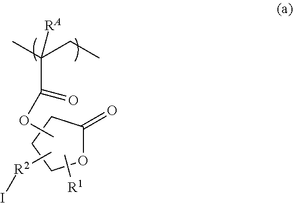
[0136]To 500 g of THF were added 110 g of 3-hydroxy-4-iodo-5-methyloxolan-2-one and 3.7 g of 4-(dimethylamino)pyridine. Under ice cooling, 92.4 g of methacrylic anhydride was added dropwise to the solution. The solution was stirred at room temperature for 5 hours. Then water was added to quench the reaction, followed by standard aqueous workup. The product was purified by silica gel column chromatography, obtaining 91 g (yield 65%) of Monomer 1.
2) Synthesis of Polymers
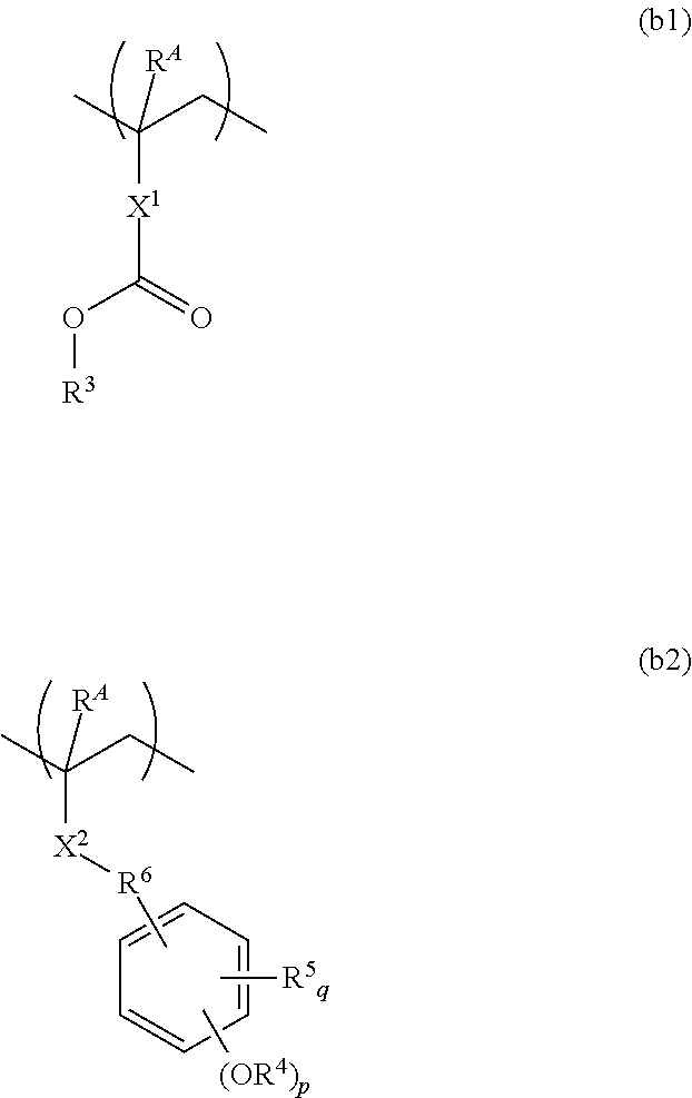
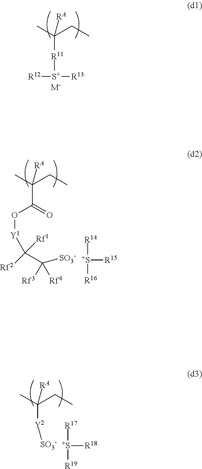
[0137]PAG Monomers 1 to 3 used in the following Synthesis Examples are identified below.
[0138]
synthesis example 2
Synthesis of Polymer 1
[0139]A 2-L flask was charged with 8.2 g of ethylcyclopentyl methacrylate, 3.6 g of 4-hydroxyphenyl methacrylate, 155 g of Monomer 1, and 40 g of THF. The reactor was cooled at −70°C in nitrogen atmosphere, after which vacuum pumping and nitrogen blow were repeated three times. The reactor was warmed up to room temperature, whereupon 1.2 g of azobisisobutyronitrile (AIBN) as polymerization initiator was added. The reactor was heated at 60° C., whereupon reaction ran for 15 hours. The reaction solution was poured into 1 L of isopropyl alcohol (IPA) whereupon white solids precipitated. The precipitate was filtered and dried in vacuum at 60° C., yielding Polymer 1.
[0140]
synthesis example 3
Synthesis of Polymer 2
[0141]A 2-L flask was charged with 5.2 g of 1-(adamantan-1-yl)-1-methylethyl methacrylate, 2.9 g of t-pentyloxystyrene, 3.6 g of 4-hydroxyphenyl methacrylate, 6.2 g of Monomer 1, 11.0 g of PAG Monomer 2, and 40 g of THF. The reactor was cooled at −70° C. in nitrogen atmosphere, after which vacuum pumping and nitrogen blow were repeated three times. The reactor was warmed up to room temperature, whereupon 1.2 g of AIBN as polymerization initiator was added. The reactor was heated at 60° C., whereupon reaction ran for 15 hours. The reaction solution was poured into 1 L of IPA whereupon white solids precipitated. The precipitate was filtered and dried in vacuum at 60° C., yielding Polymer 2.
[0142]
PUM
| Property | Measurement | Unit |
|---|---|---|
| size | aaaaa | aaaaa |
| wavelength | aaaaa | aaaaa |
| dispersity | aaaaa | aaaaa |
Abstract
Description
Claims
Application Information