Structure mounted with electronic component

a technology of electronic components and structures, applied in the direction of fixed capacitor details, printed circuit non-printed electric components association, final product manufacture, etc., can solve the problems of limiting the increase in positioning accuracy between the respective components, affecting the quality of electronic components, so as to reduce or prevent the generation of defective mounting. , the degree of mounting position accuracy is high, and the joint strength is sufficient

Active Publication Date: 2019-07-02
MURATA MFG CO LTD
View PDF26 Cites 2 Cited by
  • Summary
  • Abstract
  • Description
  • Claims
  • Application Information

AI Technical Summary

Benefits of technology

[0015]Therefore, preferred embodiments of the present invention provide a mounted structure with a high degree of mounting position accuracy and sufficient joint strength ensured while significantly reducing or preventing generation of defective mounting of an electronic component brought into a standing posture during mounting.
[0024]According to various preferred embodiments of the present invention, a mounted structure achieves a high degree of mounting position accuracy and sufficient joint strength while significantly reducing or preventing generation of defective mounting of an electronic component brought into a standing posture during mounting.

Problems solved by technology

The phenomenon is caused by the generation of an imbalance between external forces applied to the electronic component due to the surface tension of the melted solder joint material banked with wettability on each end surface of the pair of external electrodes, and caused by various factors such as misalignment of the electronic component with respect to the wiring substrate during mounting, the shifted location of the solder joint material supplied, the excessive supply of the solder joint material, and asymmetric outlines of the pair of external electrodes.
However, the phenomenon has a tendency to be caused at increased frequency as the electronic component to be mounted is reduced in size, and has become obvious as an especially large problem in extremely compact electronic components with outside dimensions of 0.5 mm or less in the height direction, the width direction, and the depth direction.
More precisely, even when the supply of the solder joint material is appropriately managed while an attempt is made to increase the outside dimension accuracy for each component, it is extremely difficult in the first place to handle extremely compact electronic components with a high degree of accuracy, there is thus a natural limit to the increased positioning accuracy between the respective components during mounting, and the frequency of the phenomenon is not able to be sufficiently reduced just by this measure.
Moreover, when the approach disclosed in JP 5-243074 A as mentioned above is adopted, firstly, a problem occurs which is that the self-alignment effect described above is significantly damaged to make misalignment likely to be caused in relation to the mounting position of the electronic component, and secondly, in the case of extremely small electronic components as described above, it is difficult in the first place to form a metallic layer on which the solder joint material is unlikely to spread with wettability, so as to cover each end surface of the pair of external electrodes.

Method used


Image

  • Structure mounted with electronic component
  • Structure mounted with electronic component
  • Structure mounted with electronic component

Examples


embodiment 1

Preferred Embodiment 1

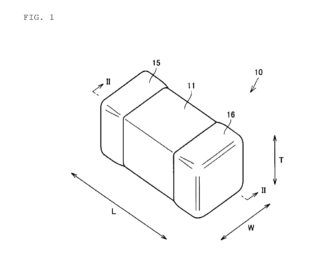
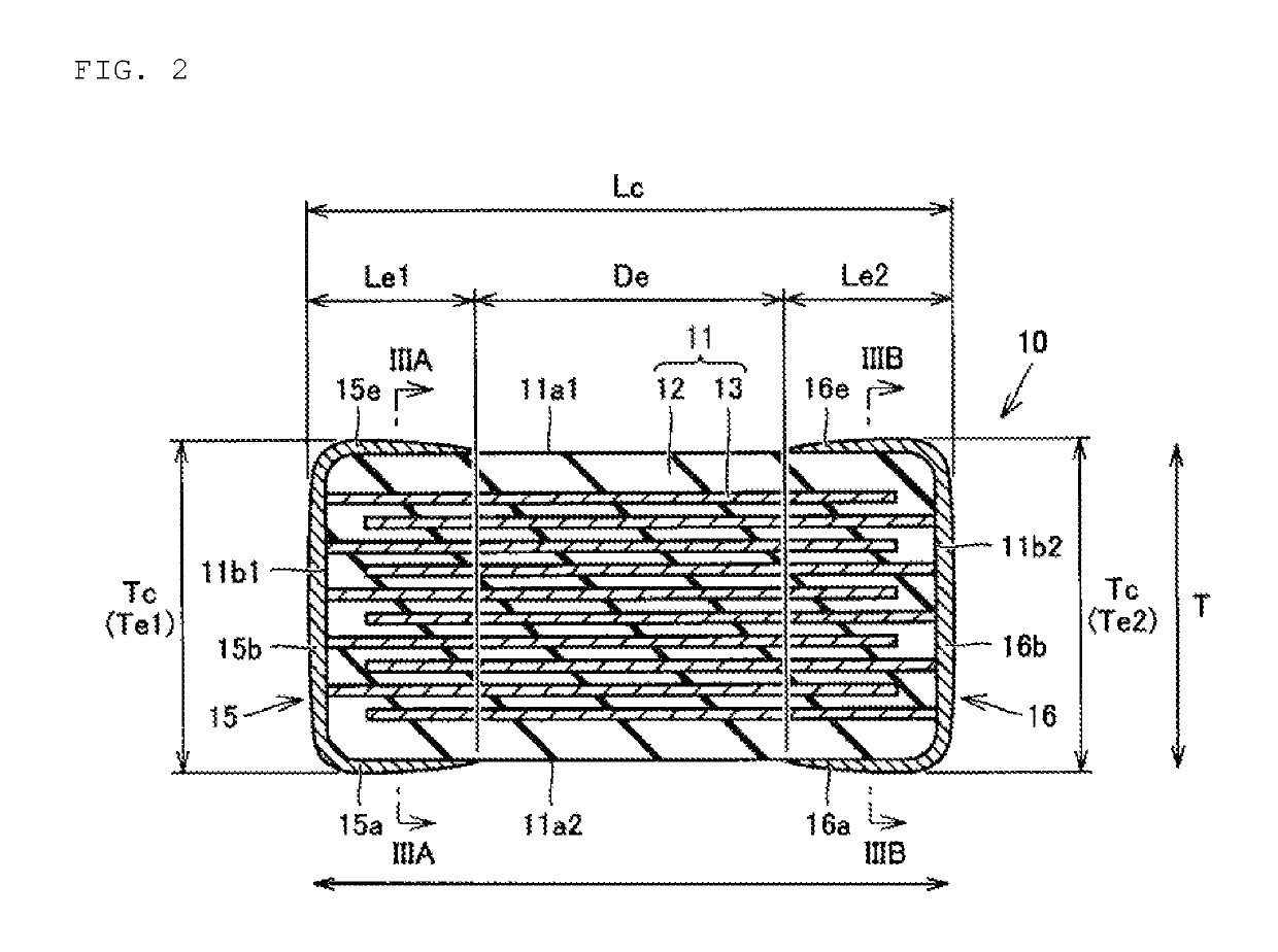
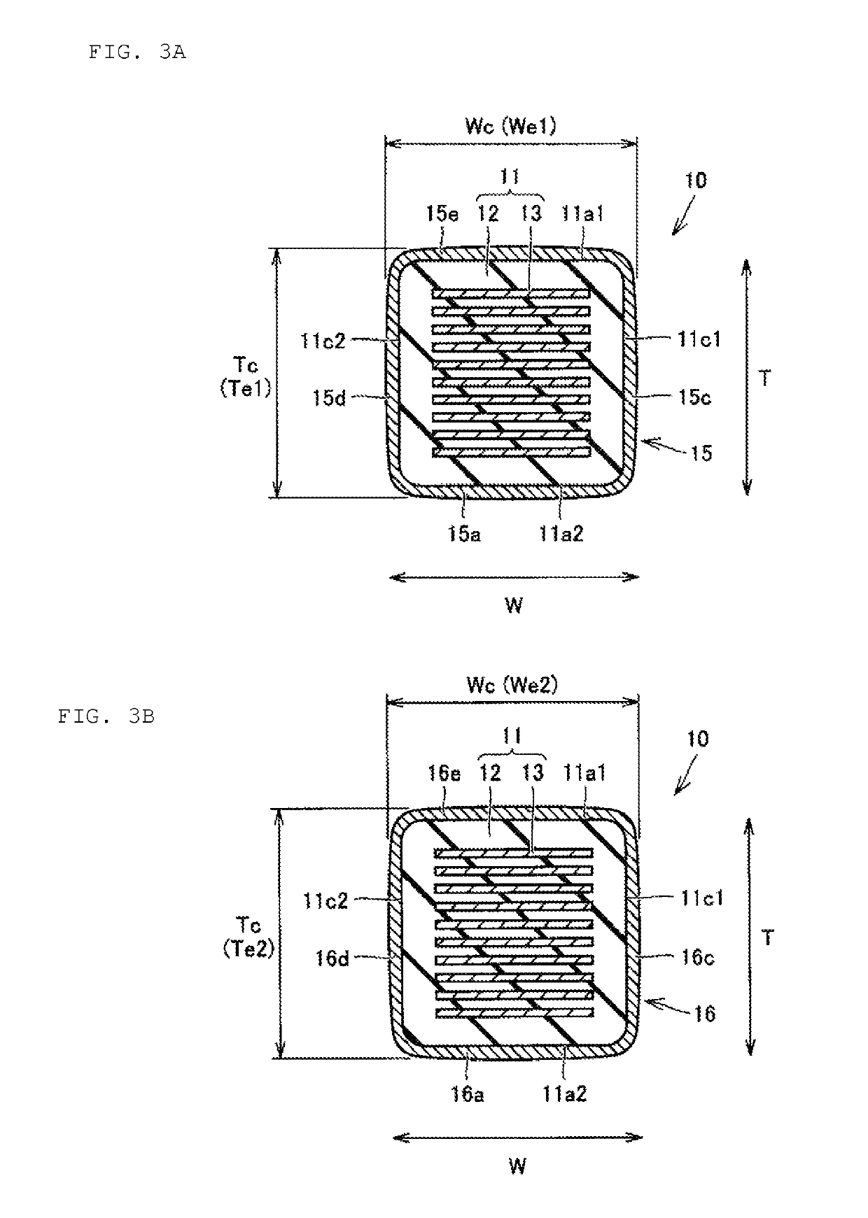
[0049]FIG. 1 is a perspective view of a laminated ceramic capacitor provided for a mounted structure in accordance with Preferred Embodiment 1 of the present invention. In addition, FIG. 2 is a schematic cross-sectional view along the line II-II shown in FIG. 1, and FIGS. 3A and 3B are schematic cross-sectional views along the line IIIA-IIIA and line IIIB-IIIB shown in FIG. 2. First, a laminated ceramic capacitor 10 provided for the mounted structure in accordance with the present preferred embodiment will be described with reference to FIGS. 1 to 3.

[0050]As shown in FIGS. 1 to 3, the laminated ceramic capacitor 10 is an electronic component which preferably has a generally rectangular or substantially rectangular parallelepiped shape, and includes a body 11, and a first external electrode 15 and a second external electrode 16 as a pair of external electrodes. It is to be noted that the rectangular or substantially rectangular parallelepiped shape also encompas...

embodiment 2

Preferred Embodiment 2

[0139]FIG. 17 is a schematic perspective view of a wiring substrate provided for a mounted structure according to the present preferred embodiment. In addition, FIG. 18 is a schematic cross-sectional view along the line XVIII-XVIII shown in FIG. 17, and FIGS. 19A and 19B are schematic cross-sectional views along the line XIXA-XIXA and line XIXB-XIXB shown in FIG. 18. Next, the wiring substrate 20B provided for the mounted structure according to the present preferred embodiment will be described with reference to FIG. 17 to FIGS. 19A and 19B.

[0140]As shown in FIGS. 17 to 18, the wiring substrate 20B, which has a generally plate-shaped configuration, is provided with a base 21, a solder resist 22, and conductive patterns 23.

[0141]The base 21 preferably is a plate-shaped and includes a pair of principal surfaces, and the solder resist 22 and conductive patterns 23 mentioned above are provided on at least one of the principal surfaces. As the material of the base 2...


PUM

PropertyMeasurementUnit
melting temperatureaaaaaaaaaa

Abstract

A mounted structure includes an electronic component including external electrodes, a wiring substrate including lands, and joint portions composed of a solder joint material and configured to join the external electrodes and the lands. The external electrodes respectively include coatings that cover a principal surface of a body, which is opposed to the wiring substrate, and coatings that cover end surfaces of the body, which are opposed to each other in the length direction. A distance De between the coatings in the length direction and a distance Dl between the lands in the length direction satisfy a condition of 0.91≤Dl / De≤1.09.

Description

BACKGROUND OF THE INVENTION[0001]1. Field of the Invention[0002]The present invention relates to a structure mounted with an electronic component (hereinafter, also referred to simply as a mounted structure), which preferably has a rectangular or substantially rectangular parallelepiped shaped electronic component mounted on a wiring substrate via a solder joint material.[0003]2. Description of the Related Art[0004]In recent years, with requested downsizing of electronic devices, electronic components typified by resistive elements, capacitor elements, and the like as passive components have been progressively reduced in size. For example, laminated ceramic capacitors as a type of capacitor element has been exponentially reduced in size, and laminated ceramic capacitors with outside dimensions in the height direction, width direction, and depth direction all below 1.0 mm have been used widely.[0005]In general, electronic components which have a pair of external electrodes provided o...

Claims


Application Information

Patent Timeline
Patent Type & Authority Patents(United States)
IPC IPC(8): H05K1/11H01G4/30H01G4/232H01G2/06H01G4/12H01G4/012H05K1/18H01G4/005H05K3/34H01G4/008H05K1/09
CPCH05K1/111H01G4/005H01G4/008H01G4/012H01G4/12H01G4/232H01G4/30H05K1/09H05K1/181H05K3/3442H01G2/065Y02P70/613H05K2201/10015H05K2201/10636H05K2201/10984H05K2203/048H05K2203/0465Y02P70/611Y02P70/50
Inventor NAKAGAWA, KIYOYUKI
Owner MURATA MFG CO LTD
Why Eureka
Try Eureka