Methods of forming source/drain contact structures on integrated circuit products

a contact structure and integrated circuit technology, applied in the field of integrated circuit fabrication, can solve the problems of reducing the performance of individual finfet devices and the overall performance of sram memory cells

Active Publication Date: 2019-08-06
GLOBALFOUNDRIES US INC
View PDF10 Cites 7 Cited by
  • Summary
  • Abstract
  • Description
  • Claims
  • Application Information

AI Technical Summary

Benefits of technology

[0006]The following presents a simplified summary of the invention in order to provide a basic understanding of some aspects of the invention. This summary is not an exhaustive overview of the invention. It is not intended to identify key or critical elements of the invention or to delineate the scope of the invention. Its sole purpose is to present some concepts in a simplified form as a prelude to the more detailed description that is discussed later.

Problems solved by technology

In turn, reducing the size of the source / drain epi semiconductor material and the conductive contact that will be formed to establish electrical contact with the source / drain region will reduce the performance of the individual FinFET devices as well as the performance of the overall SRAM memory cell.

Method used


Image

  • Methods of forming source/drain contact structures on integrated circuit products
  • Methods of forming source/drain contact structures on integrated circuit products
  • Methods of forming source/drain contact structures on integrated circuit products

Examples


Embodiment Construction

[0006]The following presents a simplified summary of the invention in order to provide a basic understanding of some aspects of the invention. This summary is not an exhaustive overview of the invention. It is not intended to identify key or critical elements of the invention or to delineate the scope of the invention. Its sole purpose is to present some concepts in a simplified form as a prelude to the more detailed description that is discussed later.

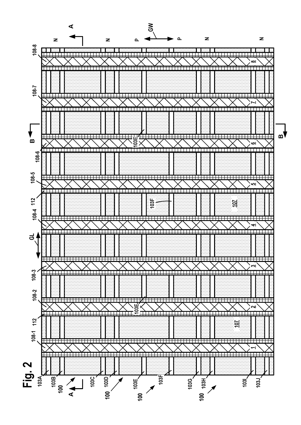
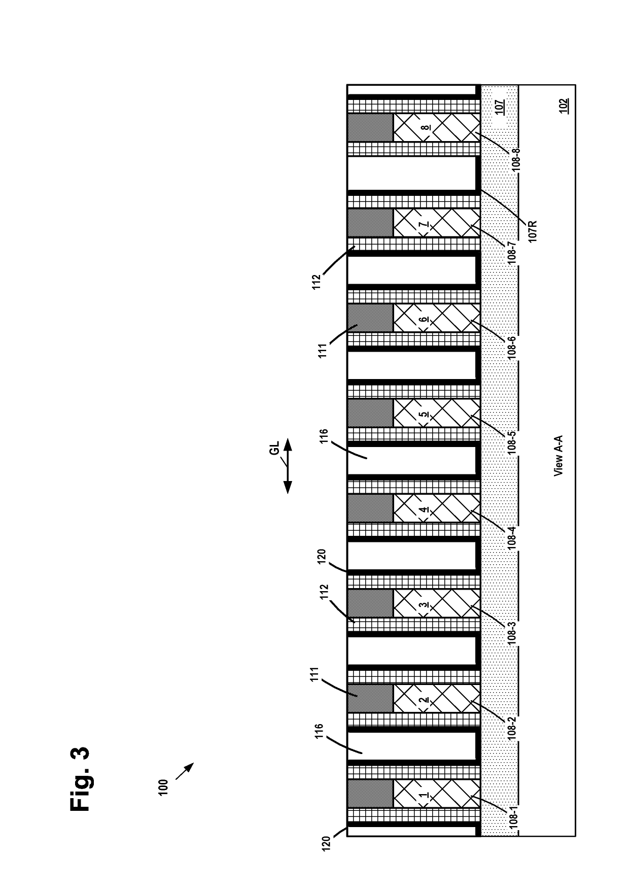
[0007]Generally, the present disclosure is directed to various methods of forming source / drain contact structures on integrated circuit products. In one illustrative example, a method disclosed herein includes forming a plurality of transistor devices on a semiconductor substrate, wherein each of the transistor devices comprises a sacrificial gate structure, a gate cap, source / drain regions, source / drain epitaxial semiconductor material in the source / drain regions, a contact etch stop layer positioned above the source / drain epitaxial ...


PUM


Abstract

One illustrative method disclosed herein includes forming a plurality of transistors on a semiconductor substrate, wherein each of the transistors comprise source/drain epitaxial semiconductor material in the source/drain regions, a contact etch stop layer (CESL) positioned above the source/drain epitaxial semiconductor material and an insulating material positioned above the contact etch stop layer, and forming a plurality of contact isolation cavities by performing at least one etching process sequence, wherein the etching process sequence is adapted to sequentially remove the insulating material, the CESL and the source/drain epitaxial semiconductor material, and forming a contact isolation structure in each of the contact isolation cavities. In this example, the method also includes, after forming the contact isolation structures, removing the sacrificial gate structures so as to form a plurality of replacement gate cavities, and forming a final gate structure in each of the plurality of replacement gate cavities.

Description

BACKGROUND OF THE INVENTION1. Field of the Invention[0001]The present disclosure generally relates to the fabrication of integrated circuits, and, more particularly, to various methods of forming source / drain contact structures on integrated circuit (IC) products and various novel IC products.2. Description of the Related Art[0002]A conventional field effect transistor (FET) is a planar device wherein the entire channel region of the device is formed parallel and slightly below the planar upper surface of a semiconducting substrate. In contrast to a planar FET, there are so-called 3D devices, such as an illustrative FinFET device, which is a three-dimensional structure. FIG. 1 is a perspective view of an illustrative prior art FinFET device 10 that is formed above a semiconductor substrate 12 wherein the fins 14 (e.g., features) of the device 10 are made of the material of the substrate 12, e.g., silicon. The device 10 includes a plurality of fin-formation trenches 13, three illustr...

Claims


Application Information

Patent Timeline
Patent Type & Authority Patents(United States)
IPC IPC(8): H01L21/8234H01L27/088H01L21/8238H01L29/66H01L21/311H01L27/092H01L21/84H01L27/12H01L21/762H01L27/108
CPCH01L21/823481H01L21/31144H01L29/66545H01L21/823431H01L21/823821H01L27/0886H01L21/823814H01L27/0924H01L27/10879H01L27/10826H01L21/76224H01L27/1211H01L21/823418H01L21/845H01L21/764H10B12/36H10B12/056
Inventor WANG, HAITINGYU, HONGZANG, HUIZHAO, WEIZHONG, YUEXU, GUOWEIECONOMIKOS, LAERTISCIAVATTI, JEROMEBEASOR, SCOTT
Owner GLOBALFOUNDRIES US INC
Why Eureka
Try Eureka