
Sputtering target for forming protective film and multilayer wiring film

a technology of protective film and wiring film, which is applied in the direction of vacuum evaporation coating, superimposed coating process, transportation and packaging, etc., can solve the problems of easy discoloration in humid atmosphere, and achieve the effect of suppressing surface discoloration, superior weather resistance, and superior etchability

Active Publication Date: 2019-10-15
MITSUBISHI MATERIALS CORP
View PDF38 Cites 0 Cited by
  • Summary
  • Abstract
  • Description
  • Claims
  • Application Information

AI Technical Summary

Benefits of technology

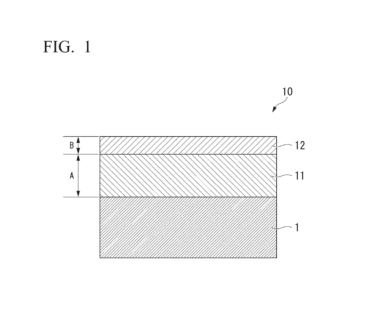
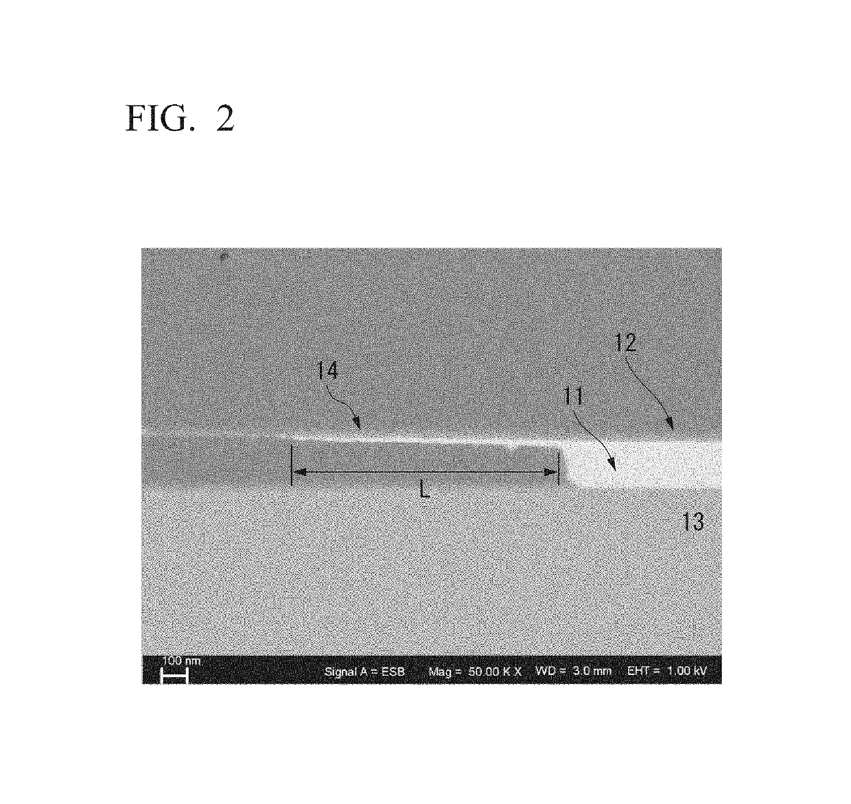
[0023]As described above, with the sputtering target for forming a protective film according) the present invention, a protective film which has superior weather resistance, can suppress surface discoloration, and has superior etchability can be formed. Further, it is possible to provide a sputtering target for forming a protective film which is formed of a copper alloy having superior hot workability; and a multilayer wiring film including a protective film that is formed using the sputtering target for forming a protective film.

Problems solved by technology

However, a Cu wiring film which is formed of copper or a copper alloy having a low specific resistance has a problem in that it easily discolors in a humid atmosphere.

Method used


Image

  • Sputtering target for forming protective film and multilayer wiring film
  • Sputtering target for forming protective film and multilayer wiring film

Examples


examples

[0068]Hereinafter, the results of an evaluation test will be described in which the effects of the sputtering target for forming a protective film and the multilayer wiring film according to the present invention were evaluated.

[0069]An ingot formed of oxygen-free copper having a purity of 99.99 mass % was prepared. By performing hot rolling, stress relief annealing, and machining on the ingot, a pure copper target for forming a Cu wiring film having an outer diameter of 100 mm and a thickness of 5 mm was prepared.

[0070]Next, a backing plate formed of oxygen-free copper was prepared. The above-described pure copper target for forming a Cu wiring film was layered on the backing plate formed of oxygen-free copper. The components were joined to each other through indium soldering at a temperature of 200° C. As a result, a target with the backing plate was prepared.

[0071]As raw materials to be melted, oxygen-free copper (purity: 99.99 mass % or higher), low-carbon nickel (purity: 99.9 m...


PUM

PropertyMeasurementUnit
temperatureaaaaaaaaaa
thicknessaaaaaaaaaa
thicknessaaaaaaaaaa

Abstract

A sputtering target is provided for forming a protective film which is used for forming a protective film on a single surface or both surfaces of a Cu wiring film, the sputtering target including 5 to 15 mass % of Ni or Ni and Al in total (where the Ni content is 0.5 mass % or higher); 0.1 to 5.0 mass % of Mn; 0.5 to 7.0 mass % of Fe; and a balance including Cu and inevitable impurities.

Description

TECHNICAL FIELD[0001]The present invention relates to a sputtering target for forming a protective film used for forming a protective film that protects a Cu wiring film formed of copper or a copper alloy; and a multilayer wiring film including a protective film that is formed using the sputtering target for forming a protective film.[0002]Priority is claimed on Japanese Patent Application No. 2013-230301, filed Nov. 6, 2013, the content of which is incorporated herein by reference.BACKGROUND ART[0003]In the related art, aluminum (Al) widely used as a wiring film of a flat panel display such as a liquid crystal panel or an organic EL panel and as a wiring film of a touch panel or the like. Recently, the size (width) and thickness of a wiring film has been reduced, and there has been a demand for a wiring film having a lower specific resistance than that in the related art.[0004]Along with the above-described reduction in the size and thickness of a wiring film, a wiring film formed ...

Claims


Application Information

Patent Timeline
Patent Type & Authority Patents(United States)
IPC IPC(8): C22C9/00C23C14/34C22C9/06C22C9/01H01J37/34C23C14/14C23C14/00C23C14/16C23C30/00C23C28/02C22C9/05
CPCC22C9/01C22C9/06C23C14/3414C22C9/00H01J37/3426Y10T428/12903Y10T428/12882Y10T428/1291C22C9/05C23C14/14C23C14/00C23C14/34C23C14/165C23C14/16C23C14/3407C23C30/00C23C28/02C23C30/005C23C28/021C23C28/023
Inventor MORI, SATORUKOMIYAMA, SHOZO
Owner MITSUBISHI MATERIALS CORP
Learn More