PEALD apparatus to enable rapid cycling

a technology of atomic layer deposition and rapid cycling, which is applied in the direction of chemical vapor deposition coating, electric discharge tube, coating, etc., can solve the problem that the cycle of more than two precursors may take longer, and achieve the effect of enhancing the formation of a film and rapid switching of precursors

Active Publication Date: 2019-11-19
APPLIED MATERIALS INC
View PDF6 Cites 1 Cited by
  • Summary
  • Abstract
  • Description
  • Claims
  • Application Information

AI Technical Summary

Benefits of technology

[0006]Embodiments described herein include a semiconductor processing chamber having a substrate support, an electrode opposite the substrate support, the electrode having a gas inlet in a peripheral region thereof, and an edge ring disposed around a peripheral region of the substrate support, the edge ring having a first barrier and a second barrier, wherein each of the first barrier and the second barrier mates with a recess in the electrode. The edge ring provides a gas flow path through a processing zone between the substrate support and the electrode that is substantially parallel to the upper surface of the substrate support. The electrode may be powered to enhance formation of a film on a substrate.
[0007]A plurality of high speed valves may be coupled to the gas inlet to provide rapid switching of precursors and / or reactants into the gas inlet.

Problems solved by technology

More complex cycles involving more than two precursors may take longer.

Method used


Image

  • PEALD apparatus to enable rapid cycling
  • PEALD apparatus to enable rapid cycling
  • PEALD apparatus to enable rapid cycling

Examples


Embodiment Construction

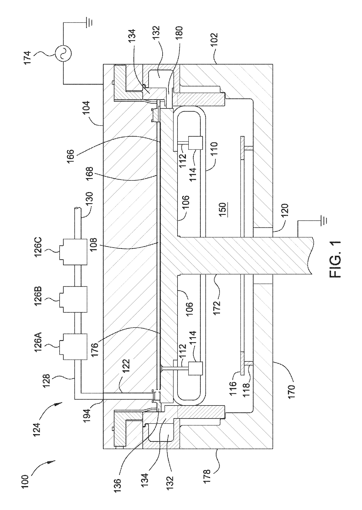
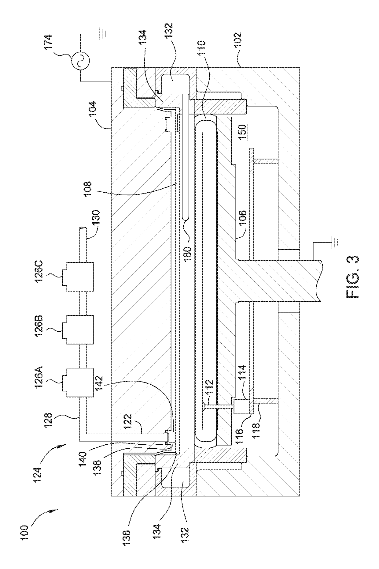
[0015]FIG. 1 is a cross-sectional view of a processing chamber 100 according to one embodiment. The processing chamber 100 has a chamber body 102 and a chamber lid 104 that couples to the chamber body 102 to define an interior 150. A substrate support 106 is disposed in the interior 150 of the chamber 100. An upper surface 166 of the substrate support 106 and a lower surface 168 of the chamber lid 104 define a processing region 108 in which a substrate disposed in a substrate contact area 176 on the upper surface 166 of the substrate support 106 is exposed to a processing environment.

[0016]Substrates enter and exit the processing chamber 100 through a substrate passage 110 in the chamber body 102. In the cross-sectional view of FIG. 1, the substrate passage 110 is behind the cross-section plane, in the “back” of the chamber 100. The substrate support 106 is movable along a longitudinal axis, for example a vertical axis, of the chamber 100 to position the substrate support 106 altern...


PUM

PropertyMeasurementUnit
angleaaaaaaaaaa
volumeaaaaaaaaaa
distanceaaaaaaaaaa

Abstract

Methods and apparatus for forming thin films are described. A semiconductor processing chamber includes a substrate support, an electrode opposite the substrate support, the electrode having a gas inlet in a peripheral region thereof, and an edge ring disposed around a peripheral region of the substrate support, the edge ring having a first barrier and a second barrier, wherein each of the first barrier and the second barrier mates with a recess in the electrode. The edge ring provides a gas flow path through a processing zone between the substrate support and the electrode that is substantially parallel to the upper surface of the substrate support. The electrode may be powered to enhance formation of a film on a substrate.

Description

CROSS-REFERENCE TO RELATED APPLICATIONS[0001]This application claims benefit of U.S. Provisional Patent Application Ser. No. 61 / 780,224, filed Mar. 13, 2013, which is incorporated herein by reference.FIELD[0002]Embodiments described herein generally relate to methods and apparatus for atomic layer deposition. More specifically, embodiments described herein provide methods and apparatus for rapid cycling in an atomic layer deposition process.BACKGROUND[0003]Atomic layer deposition is a process commonly used to form thin films in the semiconductor industry. A typical process includes positioning a substrate in a reactor and providing a first precursor to the reactor. The first precursor deposits a first species on the substrate surface until the surface is saturated with the first species, after which deposition stops. A second precursor is then provided to the chamber. The second precursor reacts with the first species lining the surface of the substrate until no more of the first sp...

Claims


Application Information

Patent Timeline
Patent Type & Authority Patents(United States)
IPC IPC(8): C23C16/509C23C16/458C23C16/455H01J37/32
CPCC23C16/509C23C16/45536C23C16/45544C23C16/45591C23C16/4585H01J37/3244H01J37/32449H01J37/32541H01J37/32715
Inventor DU BOIS, DALE R.ZHOU, JIANHUAROCHA-ALVAREZ, JUAN CARLOS
Owner APPLIED MATERIALS INC
Why Eureka
Try Eureka