Side-edge connector system providing electrical connection between devices in a manner which minimizes dedicated connection space

a connector system and side-edge technology, applied in the direction of electrical apparatus construction details, coupling device connections, electrical apparatus casings/cabinets/drawers, etc., can solve the problems of reducing the available surface area of pcbs, reducing the size of electronic devices, and restricting access to the broad planar surface. , to achieve the effect of maximizing surface area, reducing size, and thin thickness

Active Publication Date: 2020-01-14
TAG CONNECT LLC
View PDF32 Cites 21 Cited by
  • Summary
  • Abstract
  • Description
  • Claims
  • Application Information

AI Technical Summary

Benefits of technology

[0010]The present invention generally relates to devices, systems and methods for accessing devices for electrical communication. In particular, the present invention provides a connector system that utilizes a side-edge surface of a device, such as a module or printed circuit board (PCB), for connectivity. Typically, PCBs are planar, having a broad top surface and a broad bottom surface with a relatively thin thickness. This allows maximization of surface area upon which to mount electronic components. Since electronic devices are becoming smaller and smaller in size, the available surface area of PCBs is also becoming smaller. Often, there is a need to temporarily connect to PCBs for the purpose of testing or configuring circuitry, firmware, and / or software. The present invention provides for such connectivity without dedicating space on the broad planar surfaces of devices such as PCBs; this maximizes utilization of the available planar space for desired electronic components. The present invention utilizes the side-edge surface of the device along its thickness to provide connectivity. This is useful in many situations, including wherein the device, such as a PCB, is to be soldered as a part onto a larger board at a later point in time. This eliminates the need for an extra connector mounted on the device in addition to the larger board. Likewise, in some situations devices, such as PCBs, are stacked so that access to the broad planar surfaces are restricted. The present invention allows connectivity to the exposed side-edge surfaces of the PCBs.
[0018]In some embodiments, the inner edge surface includes a series of slots aligned with the plurality of electrical contacts wherein the wire of each of the plurality of electrical contacts emerges from a corresponding slot prior to curving downward toward the receiving platform, and wherein portions of the inner edge surface between each slot in the series of slots electrically isolate each of the plurality of electrical contacts from each other. In some embodiments, the receiving platform includes a plurality of grooves aligned with the series of slots, each groove configured to receive the curved portion of each of the plurality of electrical contacts so as to assist in maintaining separation and stability of the plurality of electrical contacts.
[0031]In some embodiments, the receiving platform includes a plurality of grooves aligned with the series of slots, each groove configured to receive the curved portion of each of the plurality of electrical contacts so as to assist in maintaining separation and stability of the plurality of electrical contacts.

Problems solved by technology

Since electronic devices are becoming smaller and smaller in size, the available surface area of PCBs is also becoming smaller.
Likewise, in some situations devices, such as PCBs, are stacked so that access to the broad planar surfaces are restricted.

Method used


Image

  • Side-edge connector system providing electrical connection between devices in a manner which minimizes dedicated connection space
  • Side-edge connector system providing electrical connection between devices in a manner which minimizes dedicated connection space
  • Side-edge connector system providing electrical connection between devices in a manner which minimizes dedicated connection space

Examples


Embodiment Construction

[0072]Specific embodiments of the disclosed connectors and devices, and methods for use therewith will now be described with reference to the drawings. Nothing in this detailed description is intended to imply that any particular component, feature, or step is essential to the invention.

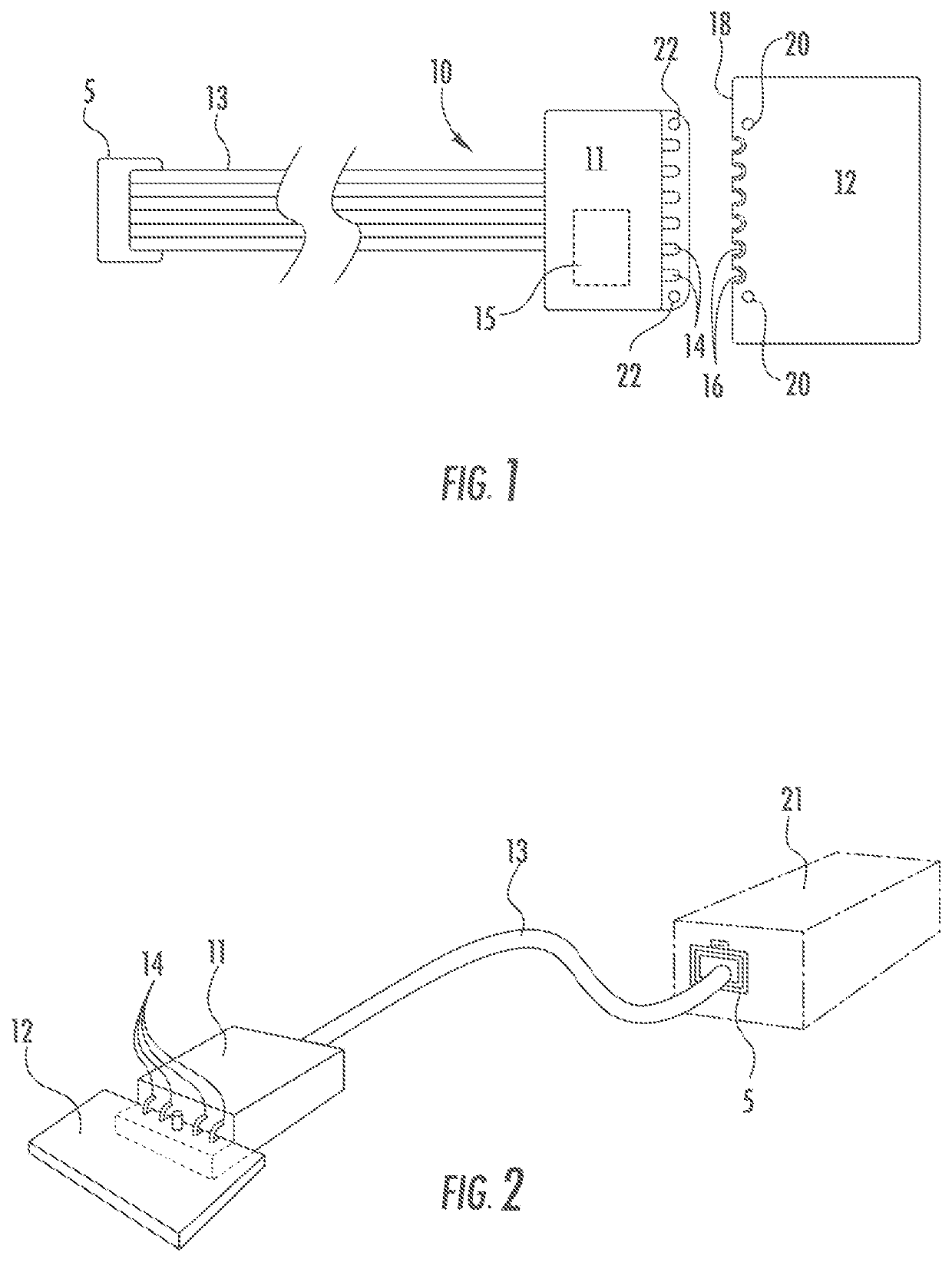
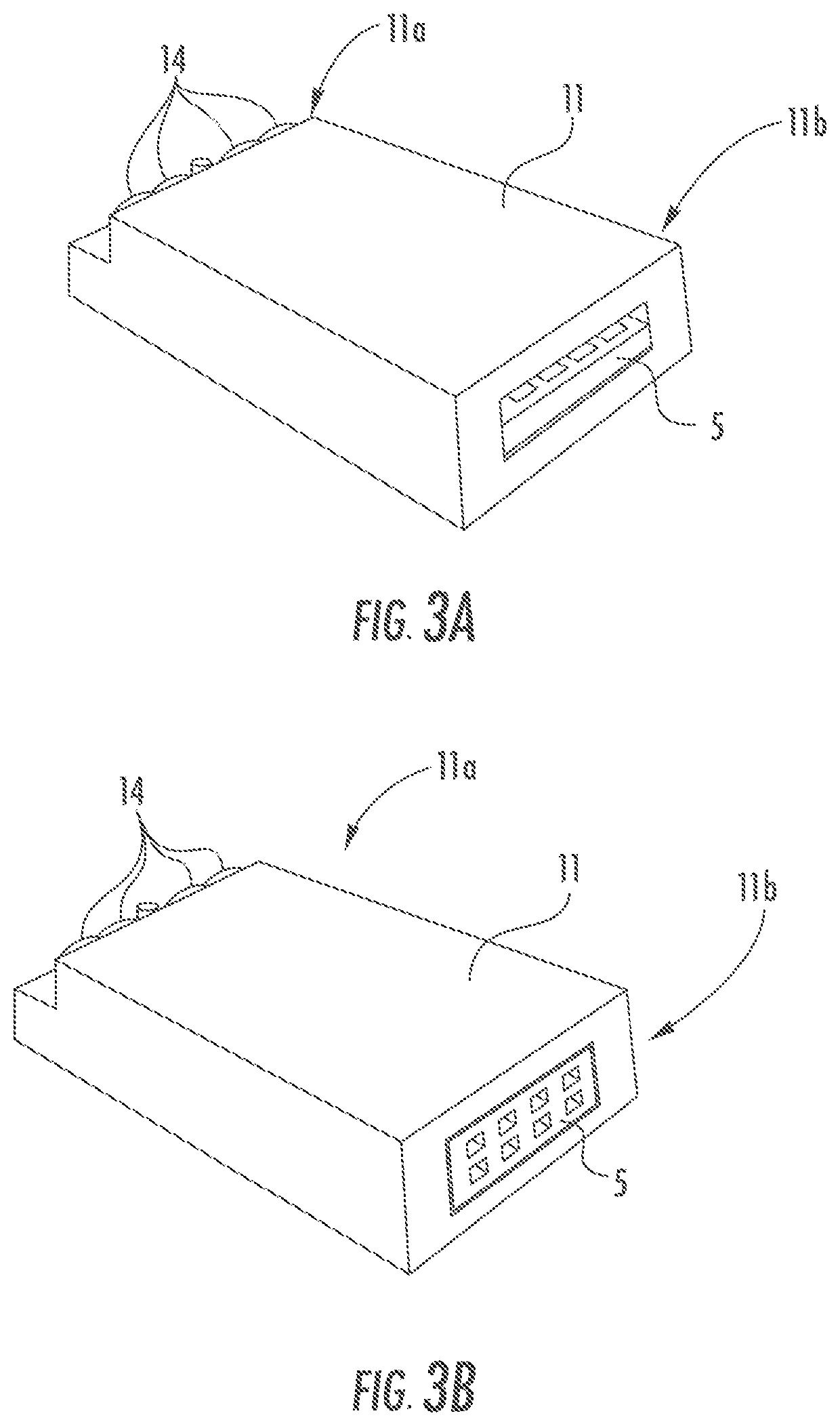
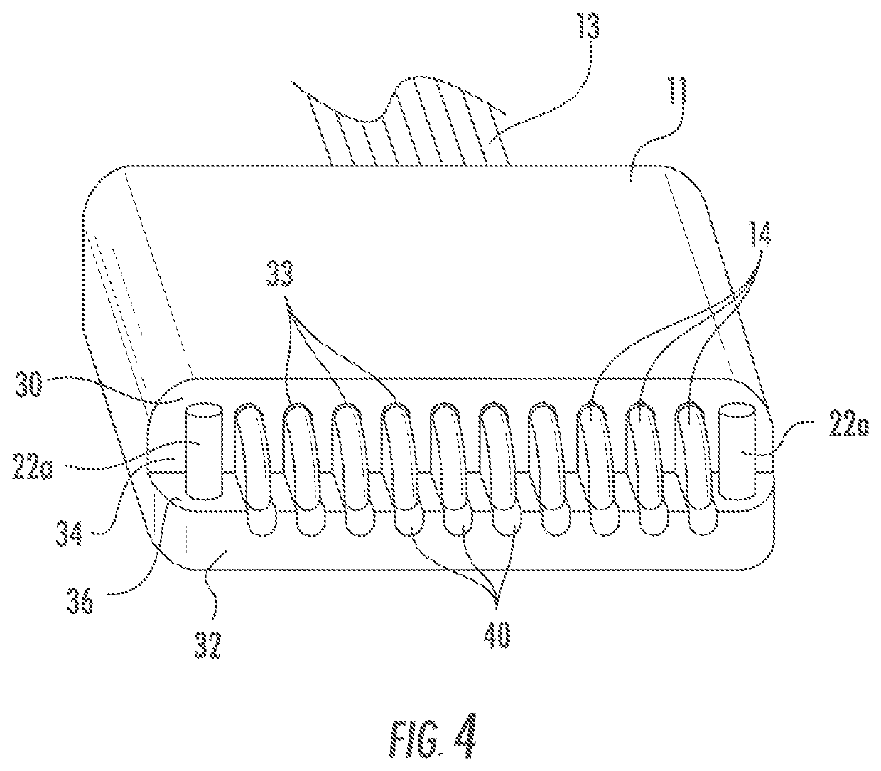
[0073]A variety of connectors are provided for making a temporary or permanent connection to a device, such as an electronic device, such as a printed circuit board (PCB), but not limited thereto. Such a connection can be made to debug, program, test, configure, monitor, inspect and / or set some state(s) of the electronic device, but is not limited thereto. Optionally the connection is used to form a debugging, programming, testing or state configuring connection between the device and an in-circuit debugger or debugger / programmer. In some embodiments, the connector has custom electronics for driving signals, for programming firmware or for wirelessly communicating with a monitoring / controlling device...


PUM


Abstract

Described herein are devices, systems and methods for accessing devices, such as modules or printed circuit boards (PCBs), for electrical communications. Various connectors described herein utilize a side-edge surface of a device, such as a PCB, for connectivity in order to maximize the surface area on the PCB upon which electronic components can be mounted. Such connectors can be used to temporarily connect to devices (e.g., PCBs) for the purposes of debugging, testing and / or configuring circuitry, firmware and / or software. Each such connector utilizes the side-edge surface of a device along its thickness to provide connectivity, which is useful in many situations, including when the device (e.g., a PCB) is to be soldered as a part onto a larger board at a later point in time, or where multiple PCBs are stacked.

Description

PRIORITY CLAIM[0001]This application claims priority to U.S. Provisional Patent Application No. 62 / 469,884 filed on Mar. 10, 2017, incorporated herein by reference for all purposes.BACKGROUND OF THE INVENTION1. Field of the Invention[0002]The present invention relates generally to connectors and more specifically it relates to connector features providing electrical connection between two devices in a manner which minimizes dedicated connection space and allows access to constrained devices.2. Description of the Background Art[0003]Any discussion of the related art throughout the specification should in no way be considered as an admission that such related art is widely known or forms part of common general knowledge in the field.[0004]Connectors, such as electrical connectors, have been in use for years and are manufactured in various configurations and styles. A variety of electrical connectors are used to provide access to the electronics on printed circuit boards.[0005]A printe...

Claims


Application Information

Patent Timeline
Patent Type & Authority Patents(United States)
IPC IPC(8): H01R12/72H05K5/00H01R13/50H01R13/627H05K7/10H01R12/71
CPCH01R12/721H05K7/1069H01R13/6273H05K5/0069H01R12/714H01R13/50H01R12/7005H01R13/665H05K1/117H05K3/325H05K3/403H01R2201/20H05K2201/09181
Inventor SHERMAN, NEIL STANLEYEASTMAN, BRIAN JOSEPH
Owner TAG CONNECT LLC
Why Eureka
Try Eureka