Elastic wave device

a technology of elastic wave and conductive film, which is applied in the direction of piezoelectric/electrostrictive/magnetostrictive devices, semiconductor devices, basic electric elements, etc., can solve the problems of metal film protruding to the lateral sides from the end edges of segmented piezoelectric substrates or reaching parts of the side surfaces, metal film may contact other conductive parts and other electronic components, and short-circuit breakdown occurs, so as to prevent physical breakage and short-cir

Active Publication Date: 2020-03-24
MURATA MFG CO LTD
View PDF38 Cites 0 Cited by
  • Summary
  • Abstract
  • Description
  • Claims
  • Application Information

AI Technical Summary

Benefits of technology

[0012]In a specific aspect of a method for manufacturing an elastic wave device according to a preferred embodiment of the present invention, in the forming of the heat dissipating film, the heat dissipating film is formed such that an outer circumferential edge of the main surface of the pair of main surfaces of the heat dissipating film at a side farther from the second main surface of the piezoelectric substrate is located in the inner side portion relative to the outer circumference of the second main surface. In this case, contact between the heat dissipating film and other portions and other components is able to be prevented more effectively.
[0030]With methods for manufacturing an elastic wave device and elastic wave devices according to various preferred embodiments of the present invention, contact between a heat dissipating film and other portions and other components is difficult to occur because a shape of the heat dissipating film is devised. Accordingly, physical breakage and short-circuit failure due to the contact are effectively prevented.

Problems solved by technology

For this reason, there is a risk that the metal film protrudes to the lateral sides from end edges of the segmented piezoelectric substrates or reaches parts of the side surfaces thereof.
WO 13 / 035819, there is a risk that the metal film may make contact with other conductive parts and other electronic components and short-circuit breakdown occurs.

Method used


Image

  • Elastic wave device
  • Elastic wave device
  • Elastic wave device

Examples


Embodiment Construction

[0043]Hereinafter, the present invention will be made clear by explaining specific preferred embodiments of the present invention with reference to the drawings.

[0044]It should be noted that respective preferred embodiments described in the specification are examples and partial replacements or combinations of components among different preferred embodiments can be made.

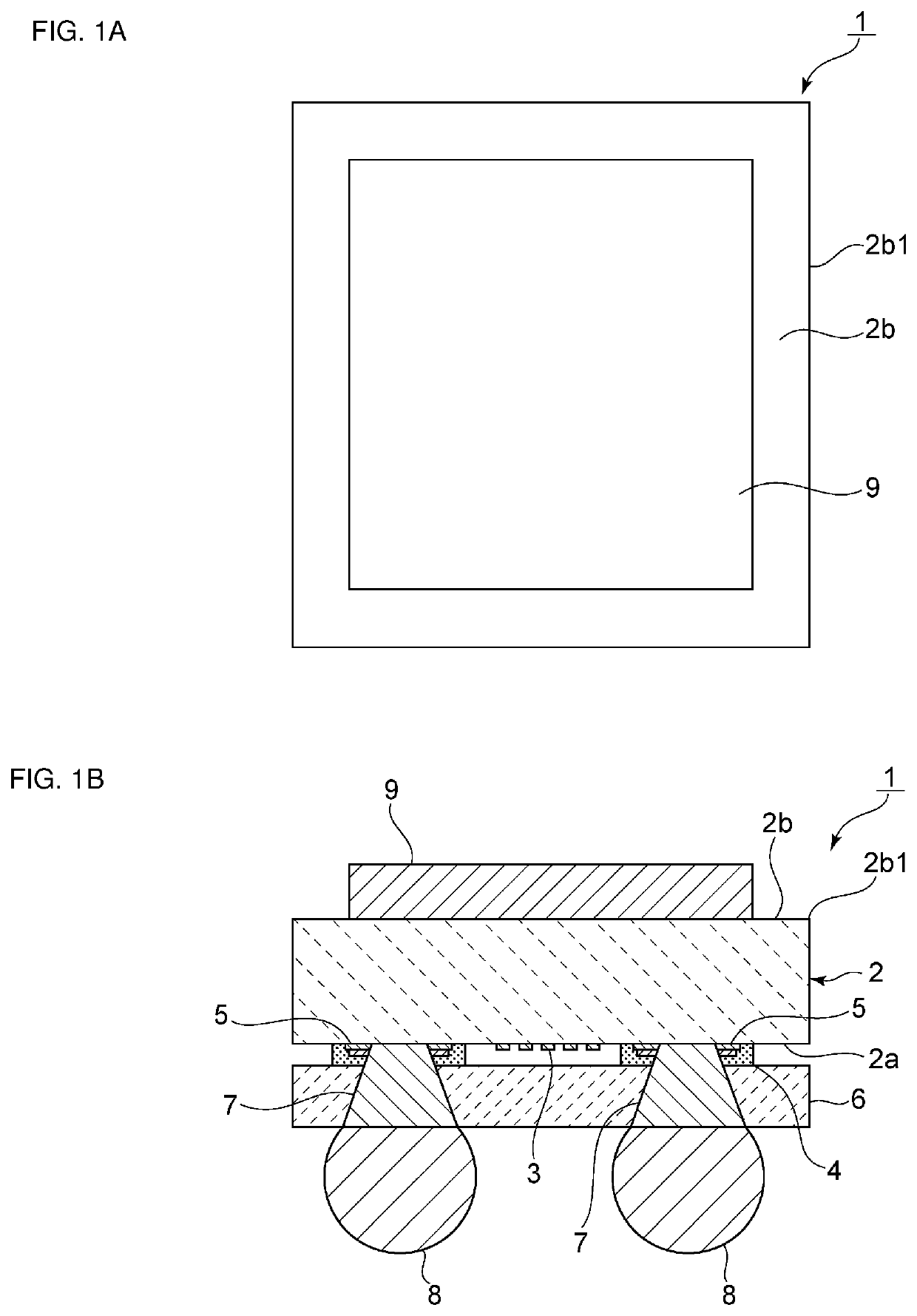
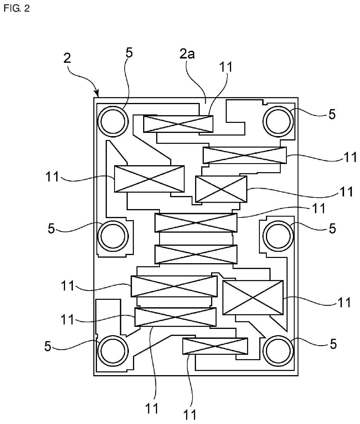
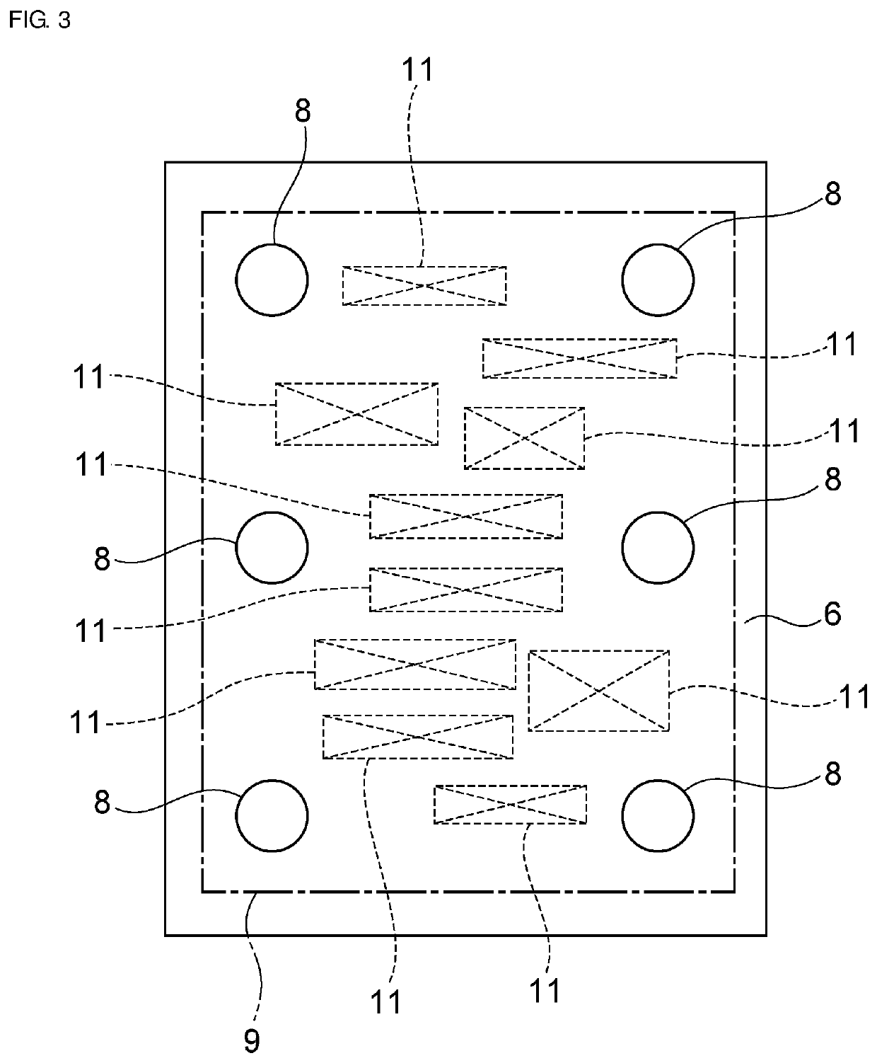
[0045]FIGS. 1A and 1B are a plan view and a schematic elevational cross-sectional view of an elastic wave device according to a first preferred embodiment of the present invention.

[0046]An elastic wave device 1 is a surface acoustic wave device including a wafer-level packaging (WLP) structure although it is not particularly limited. To be more specific, the elastic wave device 1 includes a piezoelectric substrate 2. The piezoelectric substrate 2 is made of a piezoelectric single crystal such as LiTaO3 and LiNbO3. The piezoelectric substrate 2 may be made of piezoelectric ceramics.

[0047]The piezoelectric substrate 2 ...


PUM


Abstract

An elastic wave device includes IDT electrodes on a first main surface of a piezoelectric substrate and a heat dissipating film on a second main surface and including a pair of opposing main surfaces and side surfaces connecting the pair of main surfaces. At least a portion of the side surfaces of the heat dissipating film is located in an inner side portion relative to the outer circumference of the second main surface of the piezoelectric substrate on an arbitrary cross section along a direction connecting the pair of main surfaces of the heat dissipating film.

Description

CROSS REFERENCE TO RELATED APPLICATIONS[0001]This application claims the benefit of priority to Japanese Patent Application No. 2014-245794 filed on Dec. 4, 2014 and is a Continuation Application of PCT Application No. PCT / JP2015 / 083998 filed on Dec. 3, 2015. The entire contents of each application are hereby incorporated herein by reference.BACKGROUND OF THE INVENTION[0002]1. Field of the Invention[0003]The present invention relates to a method for manufacturing an elastic wave device and the elastic wave device.[0004]2. Description of the Related Art[0005]When a surface acoustic wave device is manufactured, a mother substrate is segmented into individual piezoelectric substrates as units of electronic components. In International Publication No. WO 08 / 018452, first, a metal film is formed on the overall upper surface of a mother substrate. Then, the mother substrate on which the metal film has been formed is segmented into individual piezoelectric substrates.[0006]In Japanese Unex...

Claims


Application Information

Patent Timeline
Patent Type & Authority Patents(United States)
IPC IPC(8): H03H9/25H03H9/145H03H3/08H03H3/10H03H9/05H03H9/10H03H9/02H03H9/64H01L23/367H01L41/297H01L41/338H01L41/337H01L41/053
CPCH03H9/1071H01L41/337H03H9/059H03H9/25H01L41/297H03H9/145H03H3/10H03H9/02834H01L41/338H03H9/64H01L23/367H03H3/08H01L41/0533H01L2924/0002H01L2924/00H10N30/883H10N30/086H01L23/36H10N30/067H10N30/088
Inventor SEKIYA, DAISUKEKIKUCHI, TAKUTANAKA, HIROSHI
Owner MURATA MFG CO LTD
Why Eureka
Try Eureka