
Electrooptical device and electronic apparatus

a technology of electronic equipment and optical components, applied in the field of optical components, can solve the problems of reducing the lifetime and display performance of the electrooptical device, difficult to provide a large-sized semiconductor sensor between the display region and the signal output circuit, and achieve the effect of high sensitivity

Active Publication Date: 2020-03-31
SEIKO EPSON CORP
View PDF44 Cites 0 Cited by
  • Summary
  • Abstract
  • Description
  • Claims
  • Application Information

AI Technical Summary

Benefits of technology

The patent describes an electronic device with a display region that has dummy elements on one side. These dummy elements help to make the display look even and improve its performance. To achieve a good display, it is important to make the display region flat. This is important because the dummy elements don't appear to cause any unevenness in the display and they help to maintain the flatness of the region around the display. This results in fewer display defects and allows for better microfabrication of wiring patterns.

Problems solved by technology

As a result, display performance and a lifetime of the electrooptical device may decrease in some cases.
For this reason, it is difficult to provide a large-sized semiconductor sensor between the display region and the signal output circuit such as the data line driving circuit.
In addition, since the plurality of first signal lines or the plurality of second signal lines extend in a region along a side of the display region, it is difficult to provide a large-sized semiconductor sensor.

Method used


Image

  • Electrooptical device and electronic apparatus
  • Electrooptical device and electronic apparatus
  • Electrooptical device and electronic apparatus

Examples


first embodiment

Specific Configuration of Electrooptical Device 100

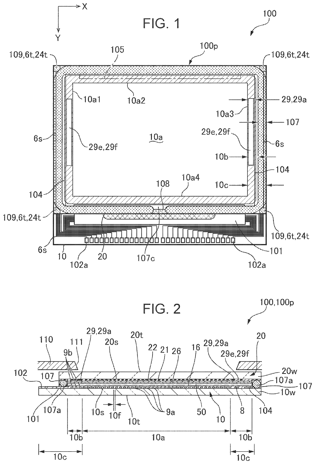
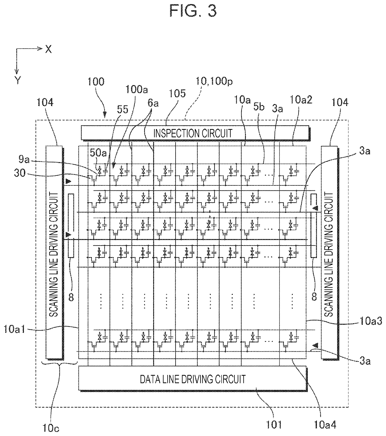
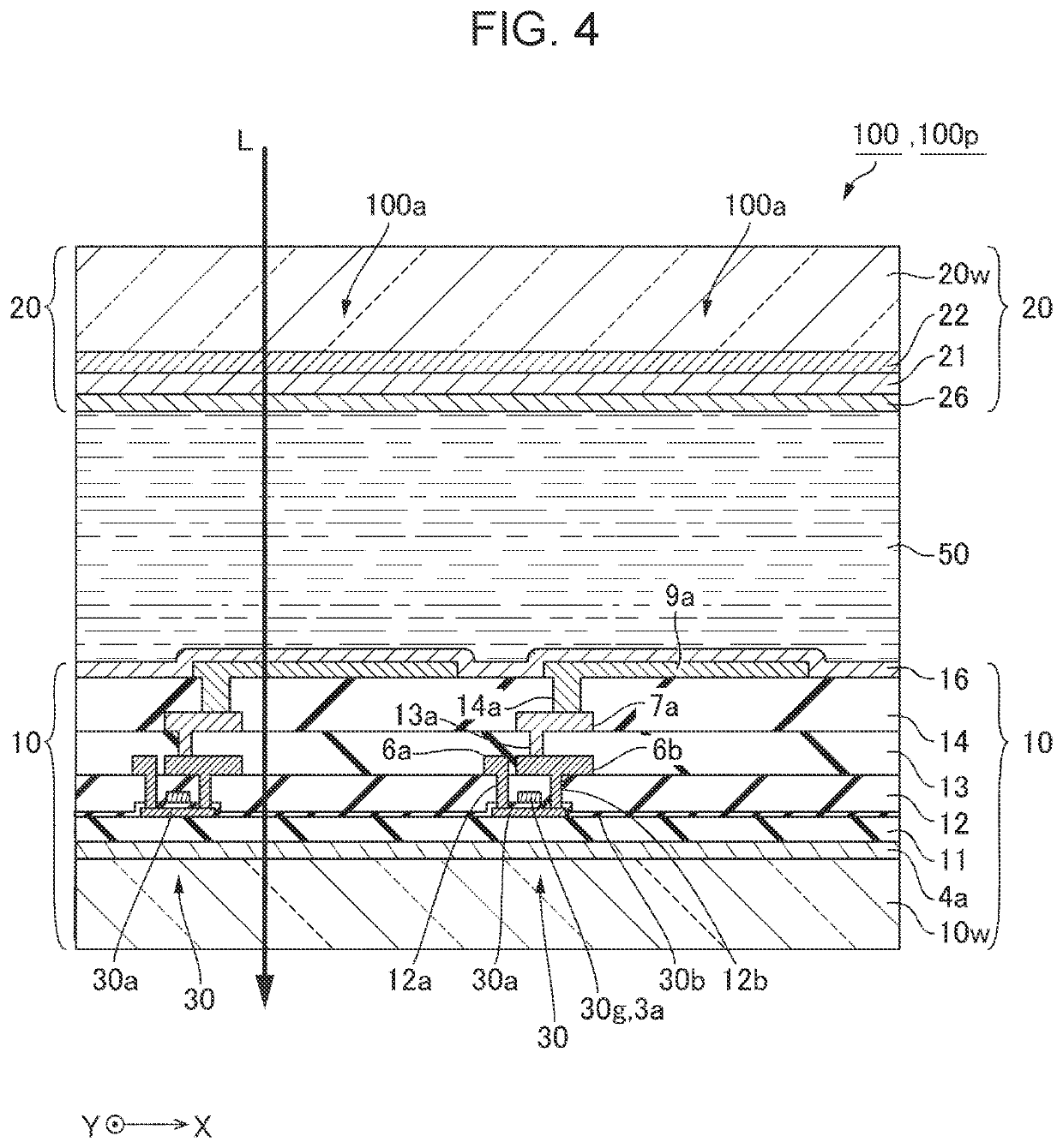
[0039]FIG. 1 is a plan view illustrating a configuration example of an electrooptical device 100 according to a first embodiment of the invention. FIG. 2 is an explanatory view schematically illustrating a section of the electrooptical device 100 illustrated in FIG. 1. The electrooptical device 100 illustrated in FIGS. 1 and 2 is a liquid crystal device, and includes a liquid crystal panel 100p. In the electrooptical device 100, a first substrate 10 and a second substrate 20 are bonded to each other by a sealing member 107 via a predetermined gap, and the sealing member 107 is provided in a frame shape along an outer edge of the second substrate 20. The sealing member 107 is an adhesive made of a photo-curable resin, a thermosetting resin, or the like, and a gap material 107a such as a glass fiber or a glass bead for keeping a distance between both substrates to a predetermined value is blended into the sealing member 107. In the li...

second embodiment

[0068]FIG. 10 is an explanatory diagram schematically illustrating a planar configuration of the semiconductor sensor 8 formed in the electrooptical device 100 according to a second embodiment of the invention. The basic configuration of the present embodiment and embodiments to be described is the same as that of the first embodiment. Thus, common portions are denoted by the same reference numerals, and a detailed description thereof will be omitted.

[0069]In the first embodiment, although the six diode elements 8b are connected to each other in series, as illustrated in FIG. 10, in the semiconductor sensor 8 (diode temperature sensor 8a) according to the present embodiment, five diode elements 8b are connected to each other in series. In addition, the scanning lines 3a linearly extend in the first direction X between the scanning line driving circuit 104 and the first side 10a1 of the display region 10a, and the sensor semiconductor layer 30s is formed between the scanning lines 3a...

third embodiment

[0070]FIG. 11 is an explanatory diagram schematically illustrating a planar configuration of the semiconductor sensor 8 formed in the electrooptical device 100 according to a third embodiment of the invention. As illustrated in FIG. 11, in the semiconductor sensor 8 (diode temperature sensor 8a) according to the present embodiment, three diode elements 8b are connected to each other in series. In addition, in a region between the scanning line driving circuit 104 and the first side 10a1 of the display region 10a, a part of the scanning line 3a is bent in the second direction Y, and then is linearly extended toward the display region 10a. In the present embodiment, the plurality of diode elements 8b are provided at a pitch of twice the wiring pitch Pa of the plurality of scanning lines 3a extending between the scanning line driving circuit 104 and the first side 10a1 of the display region 10a. Even in this case, a portion of the scanning line 3a is bent in the second direction Y, and...


PUM

PropertyMeasurementUnit
electroopticalaaaaaaaaaa
transparentaaaaaaaaaa
temperatureaaaaaaaaaa

Abstract

In an electrooptical device, a plurality of scanning lines extend between a first side of a display region and a scanning line driving circuit. A semiconductor sensor is provided between the scanning line driving circuit and the first side of the display region, the semiconductor sensor including a sensor semiconductor layer which is on the same layer as a semiconductor layer of a pixel transistor. The semiconductor sensor is a diode temperature sensor, and includes a plurality of diode elements (sensor elements) that are disposed along the first side of the display region and electrodes that electrically connect the plurality of diode elements.

Description

BACKGROUND1. Technical Field[0001]The present invention relates to an electrooptical device in which a semiconductor sensor is provided and an electronic apparatus.2. Related Art[0002]An electrooptical device such as a liquid crystal device includes a first substrate on which a pixel transistor and a pixel electrode are provided in a display region, a second substrate on which a common electrode facing the pixel electrode is provided, and an electrooptical layer which is provided between the first substrate and the second substrate, and drives the electrooptical layer between the pixel electrode and the common electrode. A parting light shielding layer is formed in a frame-shaped region on the second substrate that extends along a space between an outer edge of the display region and a sealing member. In the electrooptical device configured as described above, light-source light incident from the second substrate is modulated, and thus an image is displayed.[0003]In the electrooptic...

Claims


Application Information

Patent Timeline
Patent Type & Authority Patents(United States)
IPC IPC(8): G02F1/1368G01K7/01G02F1/1333G02F1/1362
CPCG02F1/136209G02F1/1368G01K7/01G02F1/13338G02F1/136286G02F2001/136254G02F2001/133388G02F1/133388G02F1/136254
Inventor FUJIKAWA, SHINSUKE
Owner SEIKO EPSON CORP
Learn More