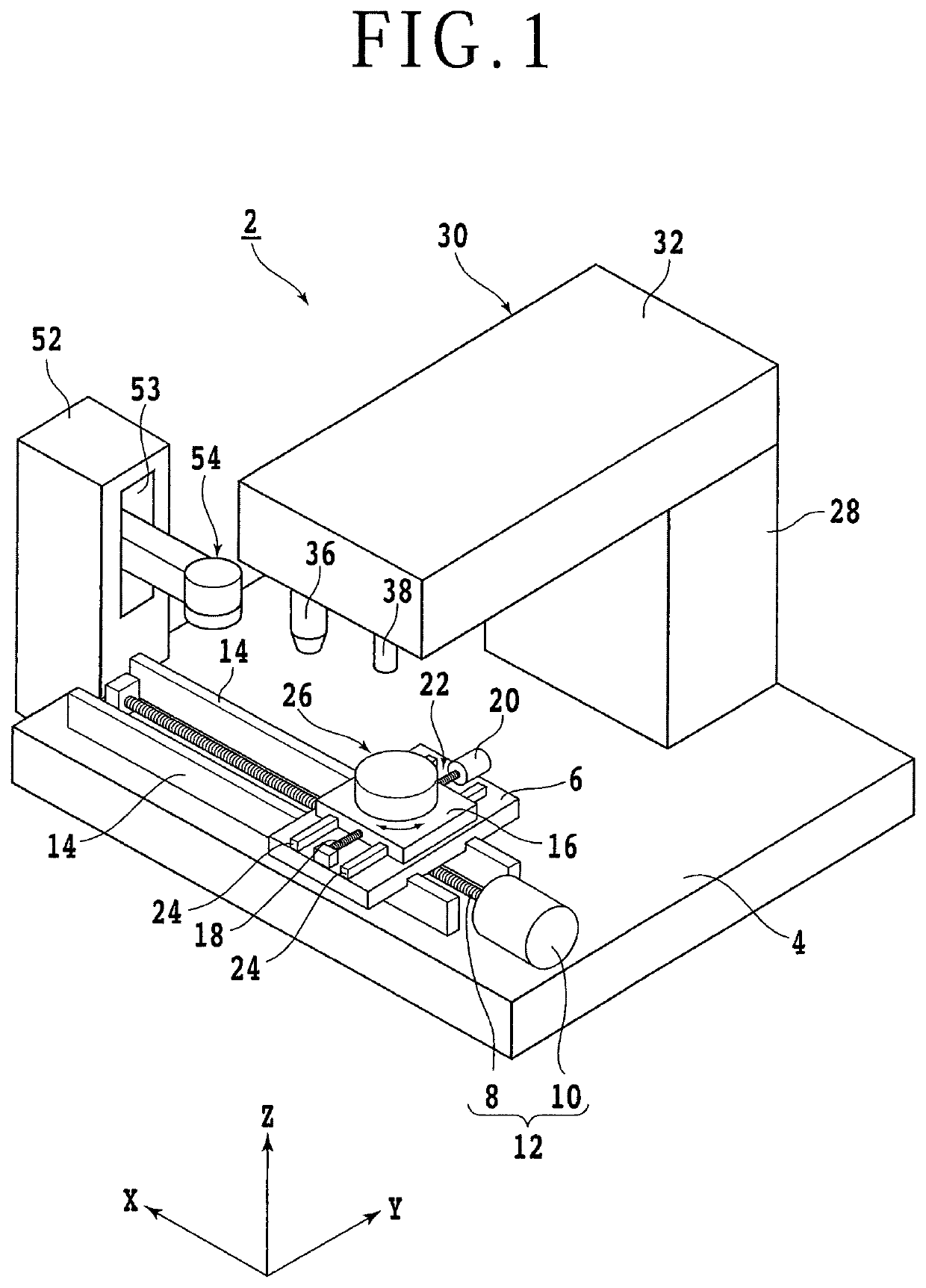
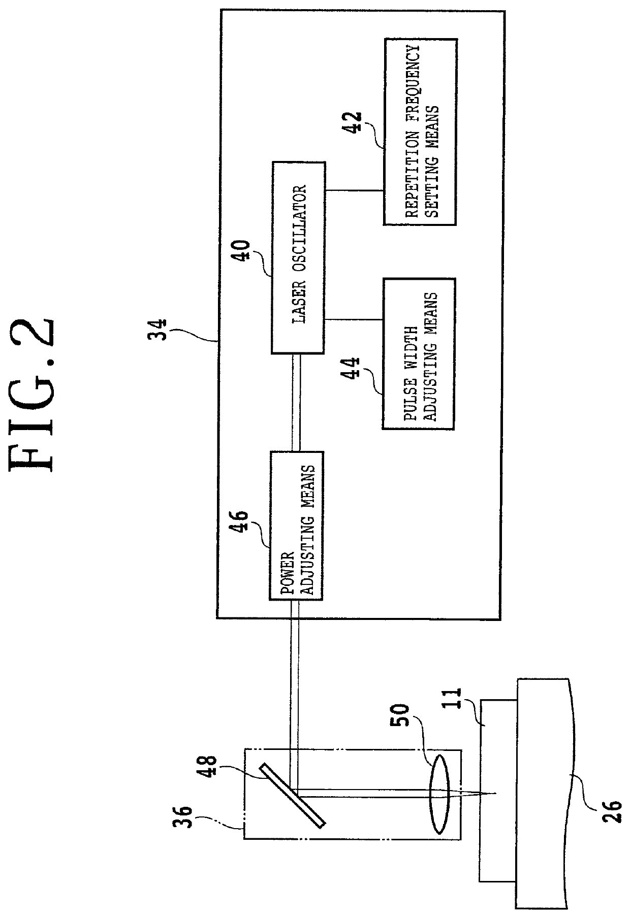
Wafer producing method
a production method and a technology of wafers, applied in the direction of polycrystalline material growth, manufacturing tools, after-treatment details, etc., can solve the problems of insufficient productivity improvement and application of very small pitch, and achieve stable crack size, easy to perform, and increase the index amount of the focal point
- Summary
- Abstract
- Description
- Claims
- Application Information
AI Technical Summary
Benefits of technology
Problems solved by technology
Method used
Image

Examples
experiment 1
[Experiment 1]
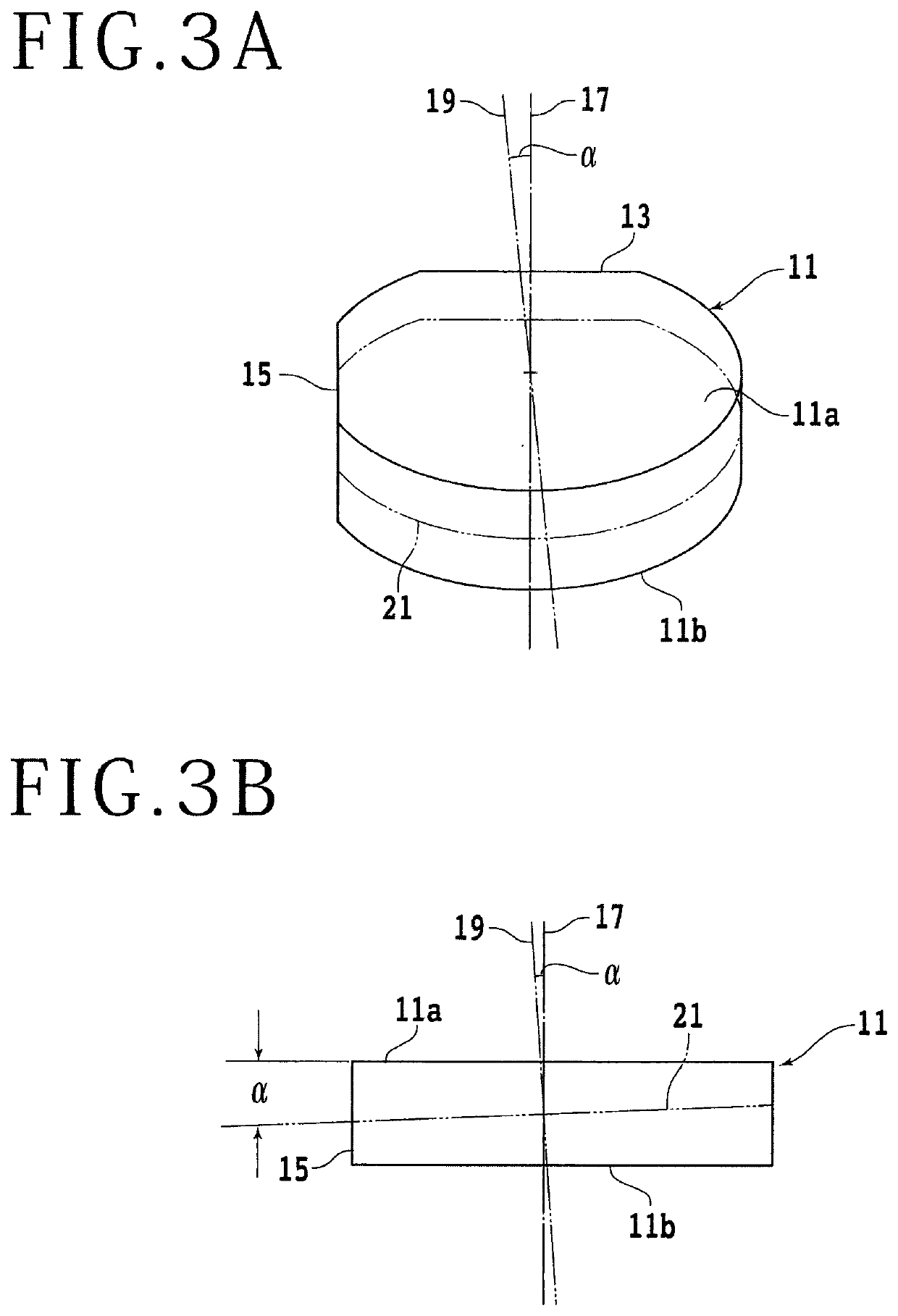
[0062]The direction of the polarization plane of the laser beam was set to the processing direction A (the direction perpendicular to the direction where the off angle is formed) to perform the modified layer forming step.
[0063]
Maximum crack (μm)Minimum crack (μm)First line358288Second line382305Third line385294Fourth line378289Fifth line380295Sixth line383305Seventh line381294Eighth line363289Ninth line375288Tenth line382290Sum376729376704
experiment 2
[Experiment 2]
[0064]The direction of the polarization plane of the laser beam was set to the direction B (the direction where the off angle is formed) perpendicular to the processing direction to perform the modified layer forming step.
[0065]
Maximum crack (μm)Minimum crack (μm)First line357278Second line432276Third line345264Fourth line342253Fifth line445295Sixth line352263Seventh line382255Eighth line452289Ninth line375263Tenth line353260Sum383526966531
experiment 3
[Experiment 3]
[0066]The direction of the polarization plane of the laser beam was set to the direction C inclined 45 degrees to the right with respect to the processing direction to perform the modified layer forming step.
[0067]
Maximum crack (μm)Minimum crack (μm)First line366299Second line319232Third line282189Fourth line365283Fifth line321222Sixth line283186Seventh line355276Eighth line332251Ninth line273165Tenth line342263Sum323823665604
PUM
| Property | Measurement | Unit |
|---|---|---|
| diameter | aaaaa | aaaaa |
| off angle | aaaaa | aaaaa |
| off angle | aaaaa | aaaaa |
Abstract
Description
Claims
Application Information
 - R&D
- Intellectual Property
- Life Sciences
- Materials
- Tech Scout
- Unparalleled Data Quality
- Higher Quality Content
- 60% Fewer Hallucinations
Browse by: Latest US Patents, China's latest patents, Technical Efficacy Thesaurus, Application Domain, Technology Topic, Popular Technical Reports.
© 2025 PatSnap. All rights reserved.Legal|Privacy policy|Modern Slavery Act Transparency Statement|Sitemap|About US| Contact US: help@patsnap.com