Polarizing film laminate comprising transparent pressure-sensitive adhesive layer and patterned transparent electroconductive layer, liquid crystal panel and organic EL panel

a technology of polarizing film and adhesive layer, applied in the direction of film/foil adhesives, polarising elements, instruments, etc., can solve the problems of poor pattern invisibility, deterioration of properties, and cost of composition itself, so as to reduce the reflection of light and suppress the interface

Active Publication Date: 2020-04-21
NITTO DENKO CORP
View PDF32 Cites 0 Cited by
  • Summary
  • Abstract
  • Description
  • Claims
  • Application Information

AI Technical Summary

Benefits of technology

[0030]In the configuration where the patterned transparent electroconductive layer is formed on an optical element, the present invention makes it possible to adjust the refractive index of the refractive index adjustment zone in the pressure-sensitive adhesive layer, with respect to the refractive indexes of the transparent electroconductive layer and the optical element, to thereby suppress the interface reflection. In addition, it becomes possible to significantly reduce reflected light which would otherwise be returned toward a viewing-side optical element, by the canceling-out effect based on a phase difference between respective ones of reflected light at the transparent electroconductive layer, reflected light at a surface of a second optical element and reflected light arising inside the pressure-sensitive adhesive layer.

Problems solved by technology

In this configuration, there is a problem that, when outside light enters from the transparent optical element which is disposed on the viewing-side, the entered light is reflected at an interface between the pressure-sensitive adhesive layer and another optical element which is disposed on a non-viewing side, and returned to the viewing side.
This problem becomes prominent particularly when an entry angle of outside light is relatively large.
In this type of display device, the problem “poor pattern invisibility” is pointed out that a pattern of the transparent electroconductive layer becomes visible from the viewing side, under the influence of internal reflection of entered light at an interface between a pressure-sensitive adhesive layer and the transparent electroconductive layer.
On the other hand, there is a problem that the composition itself becomes costly, because this technique is based on the use of a particular monomer component.
However, the technique disclosed in the Patent Document 2 requires the use of a large amount of the high refractive index material.
This causes a concern about deterioration in properties required as a pressure-sensitive adhesive, and a problem of an increase in cost.
Thus, there is another problem that the particles are hardly dispersed, causing whitish haze due to light scattering.
In this case, however, it becomes difficult to solve a problem of coloration.
However, it cannot solve most of the remaining problems pointed out in connection with the Patent Document 2.
Thus, the resulting pressure-sensitive adhesive becomes more costly than that in the Patent Document 2.

Method used


Image

  • Polarizing film laminate comprising transparent pressure-sensitive adhesive layer and patterned transparent electroconductive layer, liquid crystal panel and organic EL panel
  • Polarizing film laminate comprising transparent pressure-sensitive adhesive layer and patterned transparent electroconductive layer, liquid crystal panel and organic EL panel
  • Polarizing film laminate comprising transparent pressure-sensitive adhesive layer and patterned transparent electroconductive layer, liquid crystal panel and organic EL panel

Examples


##ventive example 1

Inventive Example 1

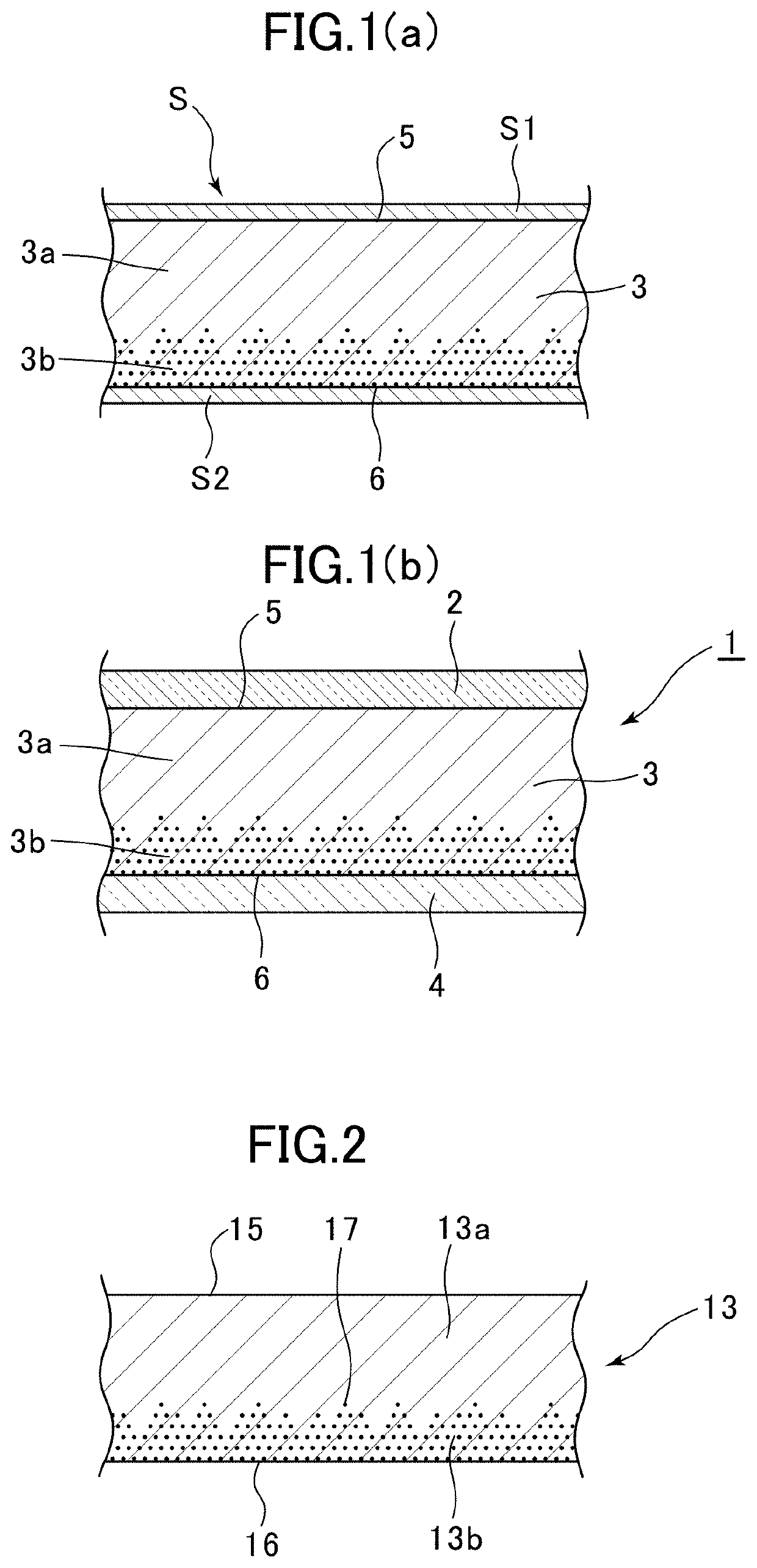
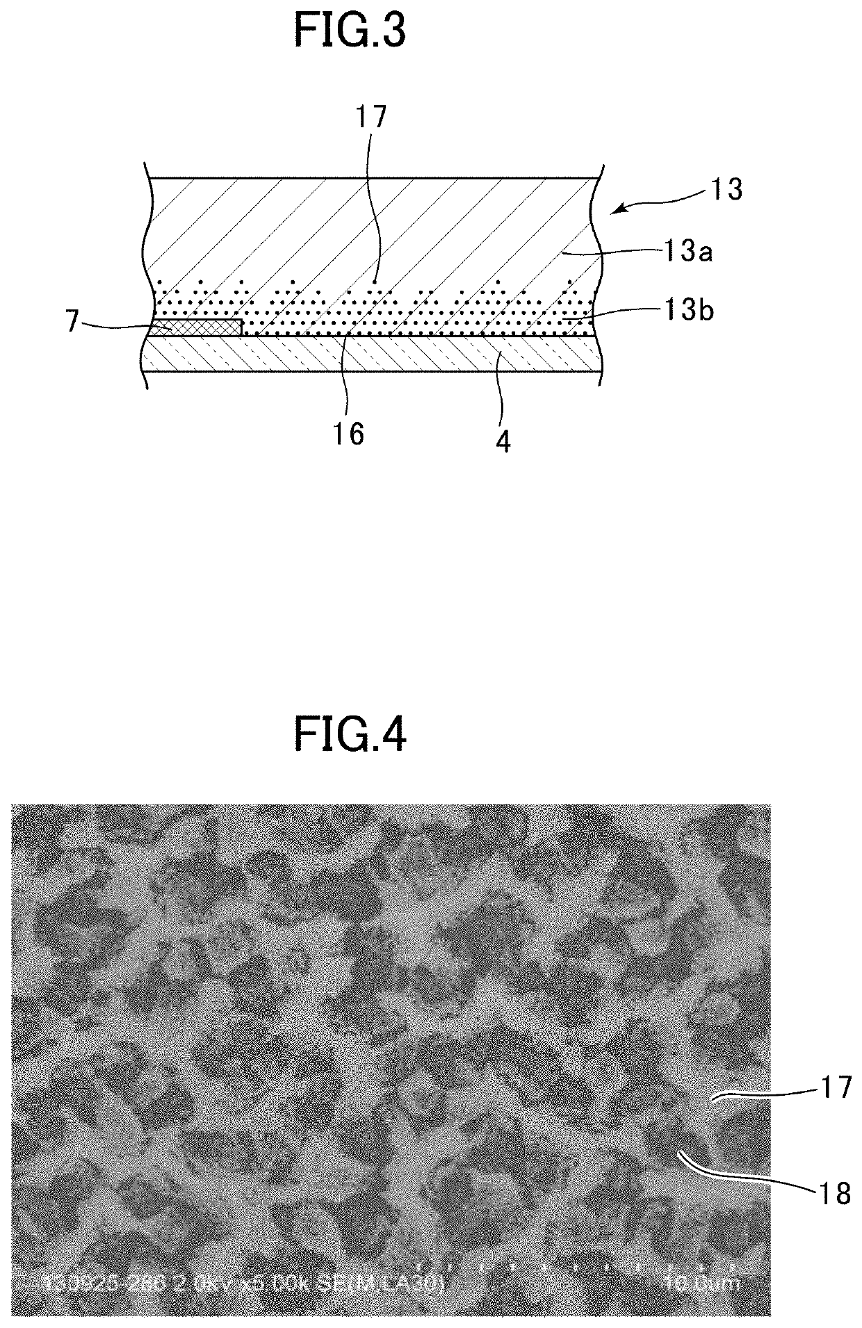
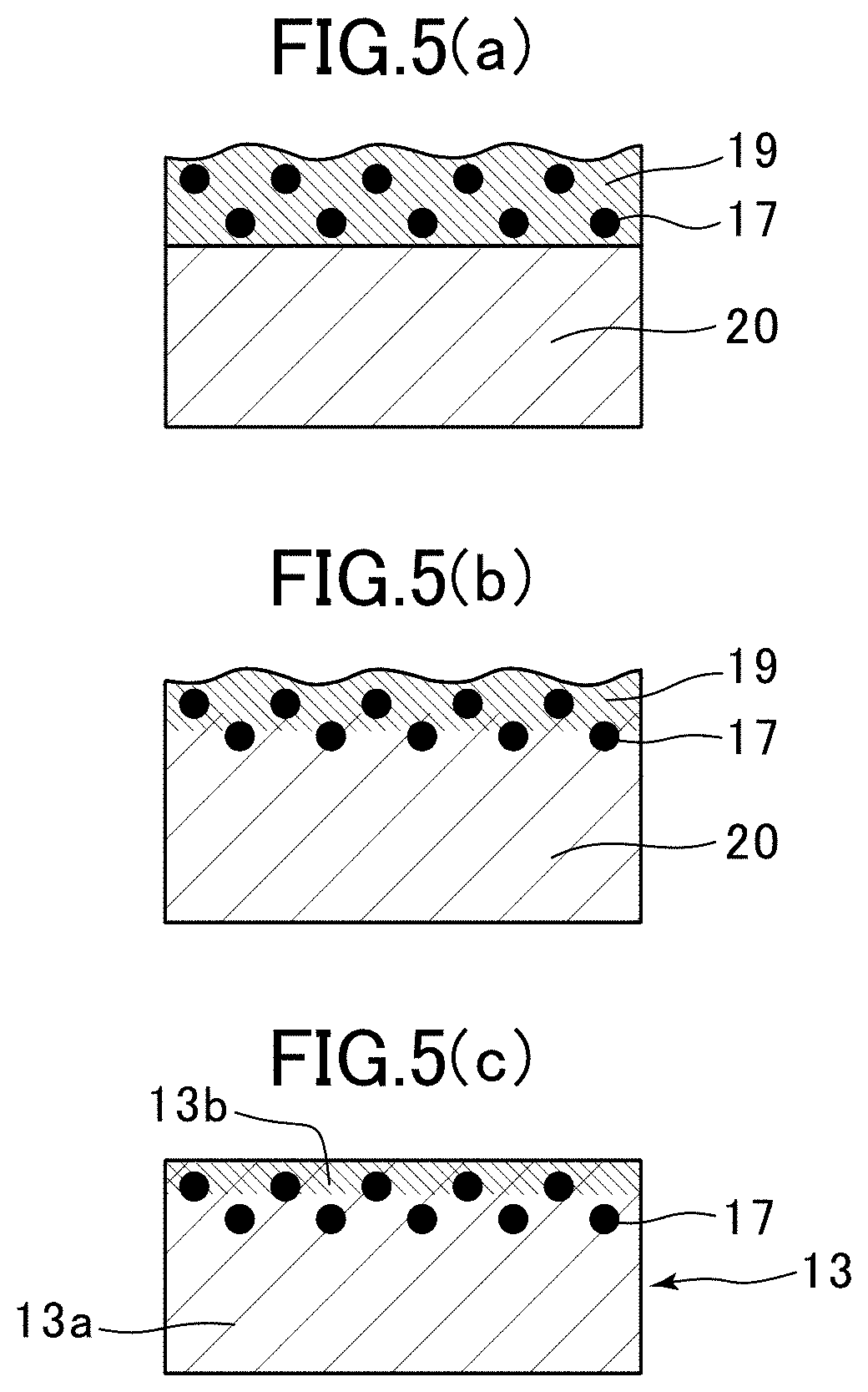
[0120]The PET separator sheet on a surface of the refractive index adjustment zone of the refractive index adjustment zone-formed pressure-sensitive adhesive layer (1) was peeled off, and the exposed surface of the refractive index adjustment zone was laminated to the patterned transparent electroconductive layer-laminated element substrate (1) of the electroconductive layer-laminated polarizing film (1), thereby producing a polarizing film laminate (A) in which the refractive index adjustment zone is in contact with the patterned transparent electroconductive layer. A configuration of the polarizing film laminate (A) in Inventive Example 1 is depicted in FIG. 9(a).

##ventive example 2

Inventive Example 2

[0121]A polarizing film laminate (B) was produced in the same manner as that in Inventive Example 1, except that a pressure-sensitive adhesive layer and an electroconductive layer-containing polarizing film to be laminated were changed, respectively, to the refractive index adjustment zone-formed pressure-sensitive adhesive layer (2) and the electroconductive layer-containing polarizing film (2), wherein the PET separator sheet on a surface of the refractive index adjustment zone of the refractive index adjustment zone-formed pressure-sensitive adhesive layer (2) was peeled off, and the exposed surface of the refractive index adjustment zone was laminated to the patterned transparent electroconductive layer-laminated element substrate (2) of the electroconductive layer-containing polarizing film (2), in such a manner that the refractive index adjustment zone is brought into contact with the patterned transparent electroconductive layer. A configuration of the pola...

##ventive example 3

Inventive Example 3

[0122]The PET separator sheet on a surface of the base adhesive zone of the refractive index adjustment zone-formed pressure-sensitive adhesive layer (2) was peeled off, and the exposed surface of the base adhesive zone was laminated to the polarizer (B-1) of the polarizing film (3). Then, the PET separator sheet on a surface of the refractive index adjustment zone of the refractive index adjustment zone-formed pressure-sensitive adhesive layer (2) was peeled off, and the exposed surface of the refractive index adjustment zone was laminated to the patterned transparent electroconductive layer-laminated element substrate (2) in such a manner that the refractive index adjustment zone is brought into contact with the patterned transparent electroconductive layer. Further, the 23 μm-thick pressure-sensitive adhesive layer A was laminated to the element substrate layer of the patterned transparent electroconductive layer-laminated element substrate layer (2) of the res...


PUM

PropertyMeasurementUnit
thicknessaaaaaaaaaa
refractive indexaaaaaaaaaa
particle sizeaaaaaaaaaa

Abstract

Provided is a polarizing film laminate comprising: an element substrate; a polarizer; a transparent electroconductive layer patterned so as to function as a touch sensor; and a pressure-sensitive adhesive layer, wherein the adhesive layer comprises: a base adhesive zone made of a transparent base pressure-sensitive adhesive material and formed over a given range from the adhesive layer in a thickness direction of the adhesive layer; and a refractive index adjustment zone formed over a given range from the adhesive layer in the thickness direction and comprising the base adhesive material and material infiltrated into the base adhesive material and different from the base adhesive material, the refractive index adjustment zone having an average refractive index greater than a refractive index of the base adhesive material, and wherein the base adhesive material zone of the adhesive layer is located on the side of the element substrate.

Description

CROSS REFERENCE TO RELATED APPLICATION[0001]This application claims the priority of Japanese Patent Application No. 2015-145288, filed on Jul. 22, 2015, in the JPO (Japanese Patent Office). Further, this application is the National Phase Application of International Application No. PCT / JP2016 / 071302, filed on Jul. 20, 2016, which designates the United States and was published in Japan. Both of the priority documents are hereby incorporated by reference in their entireties.TECHNICAL FIELD[0002]The present invention relates to a polarizing film laminate comprising a transparent pressure-sensitive adhesive layer. In particular, the present invention relates to a polarizing film laminate comprising: a transparent pressure-sensitive adhesive layer usable for bonding a transparent optical element to another optical element; and a patterned transparent electroconductive layer.BACKGROUND ART[0003]A display device such as a liquid crystal display device or an organic EL display device (OLED)...

Claims


Application Information

Patent Timeline
Patent Type & Authority Patents(United States)
IPC IPC(8): C09J7/38H01L51/52G02B5/30B32B7/02B32B7/12C09J11/04
CPCH01L51/5246B32B7/02G02B5/3083B32B7/12G02B5/3033C09J7/381C09J11/04C08K3/22C09J11/08C09J2203/318C09J2433/00C09J7/38G02F1/133502G02F2202/28C09J2301/408H10K50/844H10K50/86C09J7/20C09J201/00G02B5/30G02F1/1335B32B2307/418B32B2307/202H10K50/8426
Inventor KATAMI, HIROFUMIYASUI, ATSUSHI
Owner NITTO DENKO CORP
Why Eureka
Try Eureka