Flexible intelligent dimming film with high visible light transmittance and heat insulation and preparation method of film
An intelligent dimming and visible light technology, which is applied in optics, nonlinear optics, ion implantation plating, etc., can solve the problems of low transmittance and large-area uniformity of light-adjusting films, so as to improve visible light transmittance and suppress The effect of interface reflection
- Summary
- Abstract
- Description
- Claims
- Application Information
AI Technical Summary
Problems solved by technology
Method used
Image
Examples
preparation example Construction
[0035] The present invention also provides a method for preparing the above-mentioned flexible intelligent dimming film, comprising the following steps:
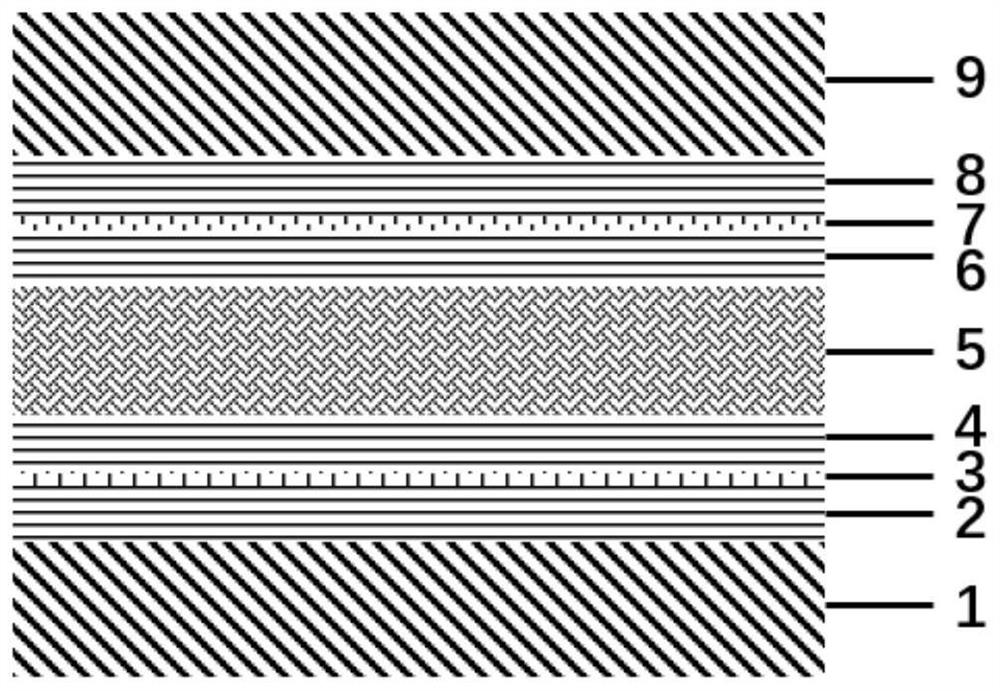
[0036]A) preparing two transparent substrates respectively, sequentially compounding an oxide layer, an ultra-thin metal layer and an oxide layer on the surface of the transparent substrates to obtain two flexible transparent conductive electrodes;
[0037] B) Coating polymer-dispersed liquid crystals on the surface of the oxide layer of the two flexible transparent conductive electrodes, superimposing them, and performing a curing reaction to obtain a flexible intelligent dimming film with high visible light transmission and heat insulation.
[0038] In the invention, two transparent substrates are firstly prepared, and then an oxide layer, an ultra-thin metal layer and an oxide layer are sequentially compounded on the surface of the transparent substrates. Among them, the composite method is not particularly limited, and a...
Embodiment 1
[0044] Step 1: Select flexible transparent PET with a thickness of 125 μm as the base layer;
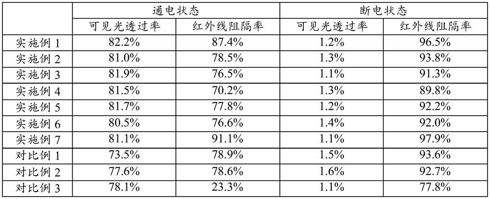
[0045] Step 2: Deposit laminated electrodes on the PET substrate by winding magnetron sputtering. Both bottom and top oxide are Nb 2 o 5 , a thickness of 20-60nm, preferably a thickness of 35nm; the metal layer is a Cu-doped Ag layer with a thickness of 6-18nm, preferably a thickness of 13nm, wherein the atomic ratio of Cu and Ag is 1:99-10:90, The preferred ratio is 5:95. Obtained PET / Nb 2 o 5 / Ag-Cu / TiO 2 The sheet resistance of the laminated electrode is 5.2Ω / sq, the average visible light transmittance (400-800nm) is 85.1% (including the substrate), and the laminated electrode has excellent mechanical flexibility;
[0046] Step 3: preparing polymer dispersed liquid crystal. Mix NOA65 UV-curable glue, LC E7 liquid crystal and silica pellets evenly, and the silica pellets with a diameter of 20 μm are used as fillers to control the thickness of PDLC devices;
[0047] Step 4: ...
Embodiment 2
[0049] Step 1: Select flexible transparent PET with a thickness of 125 μm as the base layer;
[0050] Step 2: Deposit laminated electrodes on the PET substrate by winding magnetron sputtering. Both bottom and top oxide are Nb 2 o 5 , a thickness of 20-60nm, preferably a thickness of 35nm; the metal layer is a Cu-doped Ag layer with a thickness of 6-18nm, preferably a thickness of 11nm, wherein the atomic ratio of Cu and Ag is 1:99-10:90, The preferred ratio is 5:95. Obtained PET / Nb 2 o 5 / Ag-Cu / TiO 2 The sheet resistance of the laminated electrode is 6.4Ω / sq, the average visible light transmittance (400-800nm) is 85.2% (including the substrate), and the laminated electrode has excellent mechanical flexibility;
[0051] Step 3: preparing polymer dispersed liquid crystal. Mix NOA65 UV-curable glue, LC E7 liquid crystal and silica pellets evenly, and the silica pellets with a diameter of 20 μm are used as fillers to control the thickness of PDLC devices;
[0052] Step 4: ...
PUM
| Property | Measurement | Unit |
|---|---|---|
| Thickness | aaaaa | aaaaa |
| Thickness | aaaaa | aaaaa |
| Thickness | aaaaa | aaaaa |
Abstract
Description
Claims
Application Information
 - R&D
- Intellectual Property
- Life Sciences
- Materials
- Tech Scout
- Unparalleled Data Quality
- Higher Quality Content
- 60% Fewer Hallucinations
Browse by: Latest US Patents, China's latest patents, Technical Efficacy Thesaurus, Application Domain, Technology Topic, Popular Technical Reports.
© 2025 PatSnap. All rights reserved.Legal|Privacy policy|Modern Slavery Act Transparency Statement|Sitemap|About US| Contact US: help@patsnap.com


