Pixel compensating circuit and pixel compensating method

a pixel compensating circuit and pixel compensating technology, applied in the field of display technology, can solve problems such as uneven brightness, and achieve the effect of reducing the quantum efficiency of the light emitting device and causing luminance unevenness

Active Publication Date: 2020-05-26
WUHAN CHINA STAR OPTOELECTRONICS SEMICON DISPLAY TECH CO LTD
View PDF3 Cites 0 Cited by
  • Summary
  • Abstract
  • Description
  • Claims
  • Application Information

AI Technical Summary

Benefits of technology

[0004]For solving the aforesaid technical issues, the present invention provides a pixel compensating circuit and a pixel compensating method, which can reduce the influence of the threshold voltage of the thin film transistor on the light emitting device, so that the brightness of the emitting light of the light emitting device is more uniform.
[0051]The implementation of the present invention possesses the following benefits: since the threshold voltage of the first thin film transistor is prone to drift, the magnitude of the currents flowing through different light emitting devices are different, thereby causing luminance unevenness when the light emitting device emits light. In the pixel compensating circuit of the present invention, the threshold voltage of the first thin film transistor can be compensated by the second thin film transistor. When the light emitting device emits light, the magnitude of the current flowing through the light emitting device is independent of the threshold voltage of the first thin film transistor, and the influence of factors such as the electron and hole transport efficiency in the light emitting device and the quantum efficiency of the light emitting device is reduced. Therefore, in the present invention, the influence of the first thin film transistor on the light emitting device can be neglected, so that the brightness of the different light emitting devices when emitting light is uniform.

Problems solved by technology

These factors can result in uneven brightness when different OLEDs emit light.

Method used


Image

  • Pixel compensating circuit and pixel compensating method
  • Pixel compensating circuit and pixel compensating method

Examples


Embodiment Construction

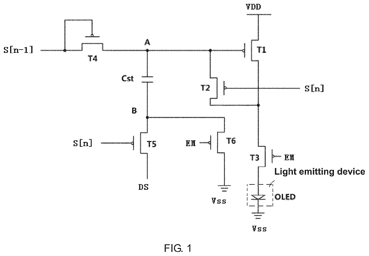
[0055]The present invention provides a pixel compensating circuit, as shown in FIG. 1, comprising a first thin film transistor T1, a second thin film transistor T2, a third thin film transistor T3, a fourth thin film transistor T4, a fifth thin film transistor T5, a sixth thin film transistor T6 and a light emitting device. Generally, the storage capacitor Cst comprises a pixel electrode and a common electrode line.

[0056]A source of the first thin film transistor T1 is connected to the constant direct current voltage signal VDD.

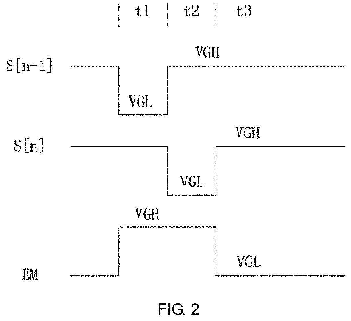
[0057]A first end of the second thin film transistor T2 is connected to a gate of the first thin film transistor T1, and a second end of the second thin film transistor T2 is connected to a drain of the first thin film transistor T1, and a third end of the second thin film transistor T2 receives a scan signal of nth stage S[n], n>1 outputted by a GOA unit of nth stage in a GOA (Gate Driver on Array) circuit.

[0058]A first end of the third thin film transistor ...


PUM

PropertyMeasurementUnit
current voltageaaaaaaaaaa
hole mobilityaaaaaaaaaa
capacitanceaaaaaaaaaa

Abstract

In the compensating circuit, a second thin film transistor (TFT) are connected to a gate and drain of a first TFT, and a source of the first TFT receives a constant DC voltage signal, and the second TFT receives a scan signal of nth stage; a third TFT is connected to the drain of the first TFT, is connected to a common ground through a light emitting device, and receives an enable signal; a fourth TFT receives a scan signal of n−1th stage, and is connected to a first end of a storage capacitor and the gate of the TFT, and a second end of the storage capacitor is connected to a fifth TFT and a sixth TFT; the fifth TFT receives a data signal and the scan signal of nth stage, respectively; the sixth TFT is connected to the common ground and receives the enable signal, respectively.

Description

CROSS-REFERENCE TO RELATED APPLICATION[0001]This application is a continuing application of PCT Patent Application No. PCT / CN2018 / 089413 entitled “Pixel compensating circuit and pixel compensating method”, filed on May 31, 2018, which claims priority to Chinese Patent Application No. 201810350263.3, filed on Apr. 18, 2018, both of which are hereby incorporated in its entireties by reference.FIELD OF THE INVENTION[0002]The present invention relates to a display technology field, and more particularly to a pixel compensating circuit and a pixel compensating method.BACKGROUND OF THE INVENTION[0003]In the display area of the AMOLED (Active-matrix organic light emitting diode) display device, the pixels are arranged in an array comprising multiple rows, multiple columns. Each pixel generally utilizes a pixel circuit comprising two thin film transistors and one capacitor for performing driving, i.e. the 2T1C driving. This 2T1C design is sensitive to the following factors: threshold voltag...

Claims


Application Information

Patent Timeline
Patent Type & Authority Patents(United States)
IPC IPC(8): G09G3/3225G09G3/3266
CPCG09G3/3225G09G3/3266G09G2320/0626G09G3/3233G09G2300/0819G09G2300/0842G09G2300/0861G09G2320/045
Inventor WANG, YIYIWANG, SHAOBO
Owner WUHAN CHINA STAR OPTOELECTRONICS SEMICON DISPLAY TECH CO LTD
Why Eureka
Try Eureka