
Controlling dimensions of a negative capacitance layer of a gate stack of a field-effect transistor (FET) to increase power density

a field-effect transistor and negative capacitance layer technology, applied in the field of field-effect transistors, can solve the problems of increasing the size of the mosfet, and achieve the effects of increasing power density, negative capacitance, and reducing the amount of charg

Active Publication Date: 2020-07-14
QUALCOMM INC
View PDF11 Cites 0 Cited by
  • Summary
  • Abstract
  • Description
  • Claims
  • Application Information

AI Technical Summary

Benefits of technology

This approach effectively increases the drain-to-source current and power density of FETs, achieving high power density in a compact form factor by precisely managing the dimensions of the negative capacitance layer.

Problems solved by technology

However, increasing the amount of surface area of the insulation layer 118 in contact with the gate electrode 130 can increase the size of the MOSFET 100 itself, which may be undesirable due to scaling preferences.

Method used


Image

  • Controlling dimensions of a negative capacitance layer of a gate stack of a field-effect transistor (FET) to increase power density
  • Controlling dimensions of a negative capacitance layer of a gate stack of a field-effect transistor (FET) to increase power density
  • Controlling dimensions of a negative capacitance layer of a gate stack of a field-effect transistor (FET) to increase power density

Examples


Embodiment Construction

[0024]With reference now to the drawing figures, several exemplary aspects of the present disclosure are described. The word “exemplary” is used herein to mean “serving as an example, instance, or illustration.” Any aspect described herein as “exemplary” is not necessarily to be construed as preferred or advantageous over other aspects.

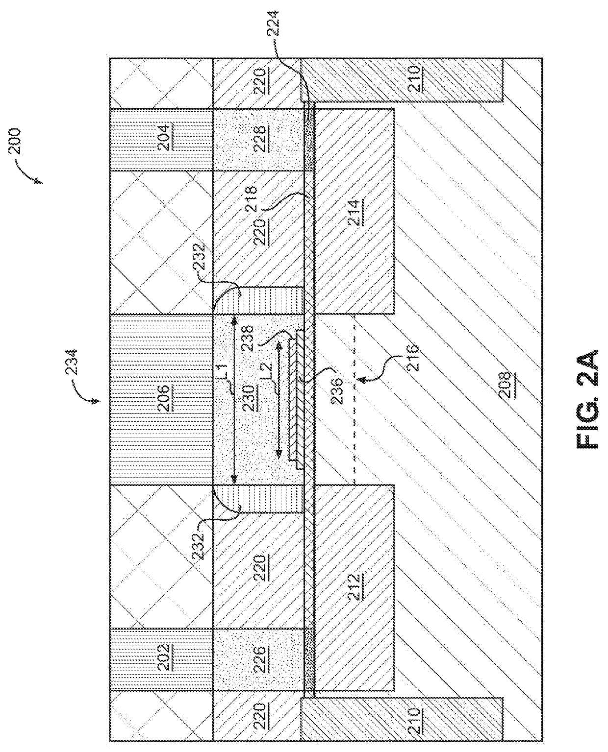
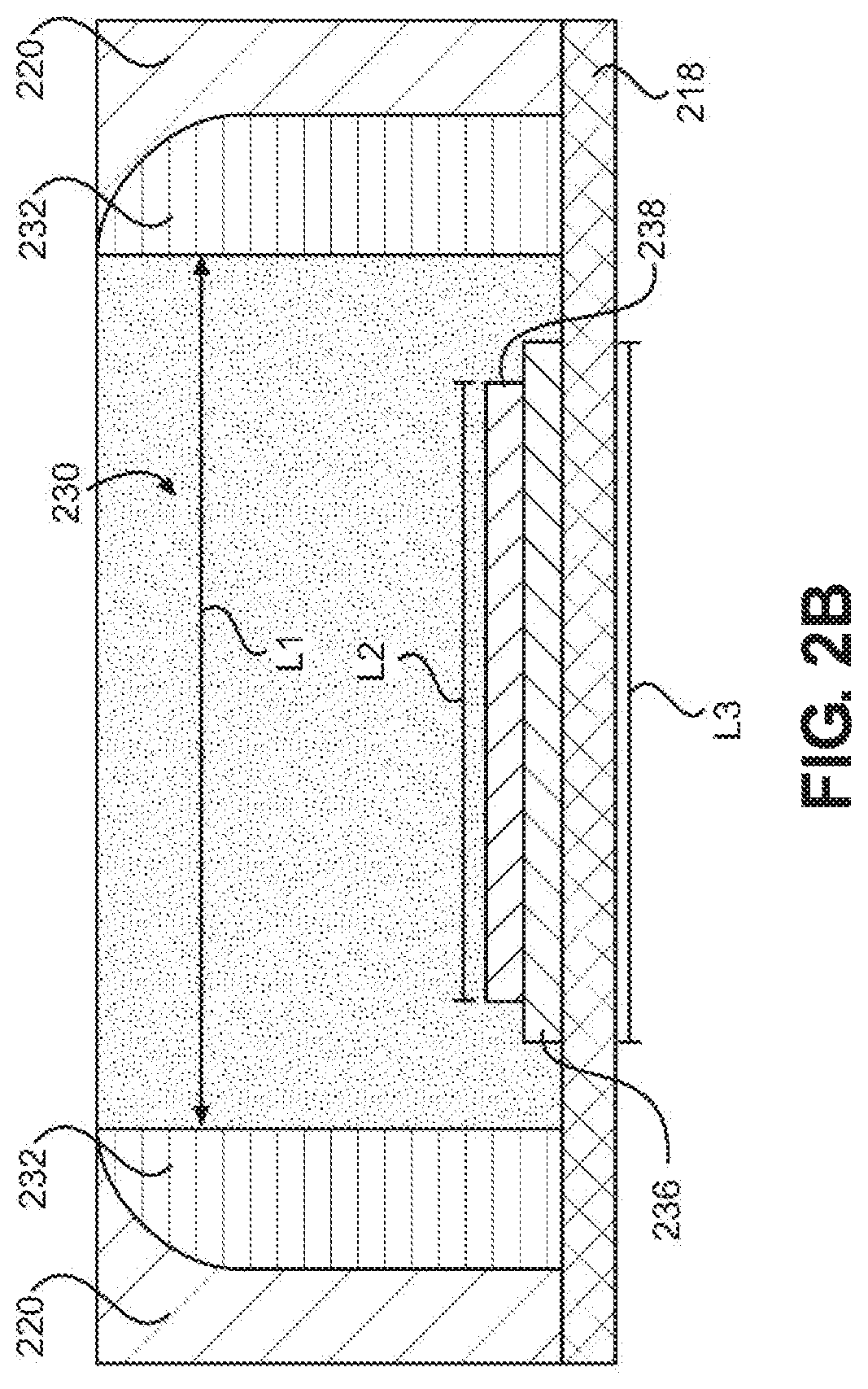
[0025]Before discussing embodiments related to controlling dimensions of a negative capacitance layer of a gate stack of a Field-Effect Transistor (FET) to increase power density, capacitance is discussed generally to provide a background for negative capacitors. A discussion of exemplary aspects of the present disclosure begins below with reference to FIG. 2A.

[0026]Generally, capacitors include a dielectric material between two plates, upon which charge can accumulate. The capacitance of a given capacitor is the rate of increase of charge with voltage. Thus, in a conventional capacitor, charge increases on each plate of the capacitor as voltage incre...


PUM

PropertyMeasurementUnit
lengthaaaaaaaaaa
lengthaaaaaaaaaa
lengthaaaaaaaaaa

Abstract

A Field-Effect Transistor (FET) with a negative capacitance layer to increase power density provides a negative capacitor connected in series with a conventional positive capacitor. The dimensions of the negative capacitor are controlled to allow the difference in capacitances between the negative capacitor and the positive capacitor to approach zero, which in turn provides a large total capacitance. The large total capacitance provides for increased power density.

Description

BACKGROUNDI. Field of the Disclosure[0001]The technology of the disclosure relates generally to Field-Effect Transistors (FETs) and, more particularly, to negative capacitance materials in gates of FETs.II. Background[0002]Field-Effect Transistors (FETs), such as metal-oxide-semiconductor (MOS) FETs (MOSFETs), are switching devices commonly used in a wide array of applications. For example, silicon (Si)-based MOSFETs are often used in high-frequency applications, such as computer logic, and in high-power applications, such as radio frequency (RF) communication devices.[0003]In this regard, FIG. 1 illustrates a conventional Si-based MOSFET 100. The conventional Si-based MOSFET 100 is a three-terminal device that includes a source 102, a drain 104, and a gate 106 over a p-type substrate 108 between two shallow trench isolation (STI) regions 110. The substrate 108 includes an n-type source region 112 under the source 102 and an n-type drain region 114 under the drain 104. The substrate...

Claims


Application Information

Patent Timeline
Patent Type & Authority Patents(United States)
IPC IPC(8): H01L29/66H01L29/49H01L29/423G11C11/22H01L29/51H01L29/78
CPCG11C11/223H01L29/7816H01L29/66689H01L29/78391H01L29/6684H01L29/4966H01L29/516H01L29/42376H01L21/28088H01L29/0878H01L29/1083H01L29/408H01L29/42368H01L29/4983H01L29/513H01L29/518H01L29/6653H01L29/66553H01L29/78
Inventor YANG, BINLU, YEGE, LIXIN
Owner QUALCOMM INC
Learn More