
Micro light emitting device and display apparatus

a light-emitting device and light-emitting device technology, applied in the direction of electrical devices, semiconductor devices, semiconductor/solid-state device details, etc., can solve the problems of shortening the spacing between two electrode pads and increasing the chances of producing defective products, and achieve good transferring success rate

Active Publication Date: 2020-10-27
PLAYNITRIDE DISPLAY CO LTD
View PDF8 Cites 0 Cited by
  • Summary
  • Abstract
  • Description
  • Claims
  • Application Information

AI Technical Summary

Benefits of technology

The invention provides a micro light emitting device and a display apparatus with good transferring success rate and production yield. The device includes a protruding structure that prevents bonding pads from conducting with each other during the transfer bonding process, which improves the yield of the display apparatus and allows for larger design margin of the micro light emitting device.

Problems solved by technology

However, the miniaturization of the LED also results in the shortening of the spacing between two electrode pads.
Consequently, during the bonding process of transferring the micro light emitting device to the display apparatus, the problem of short circuit is easy to occur due to the overflowing of the conductive soldering materials respectively connected to the two electrode pads, thereby increasing the chances of producing defective products.

Method used


Image

  • Micro light emitting device and display apparatus
  • Micro light emitting device and display apparatus
  • Micro light emitting device and display apparatus

Examples


Embodiment Construction

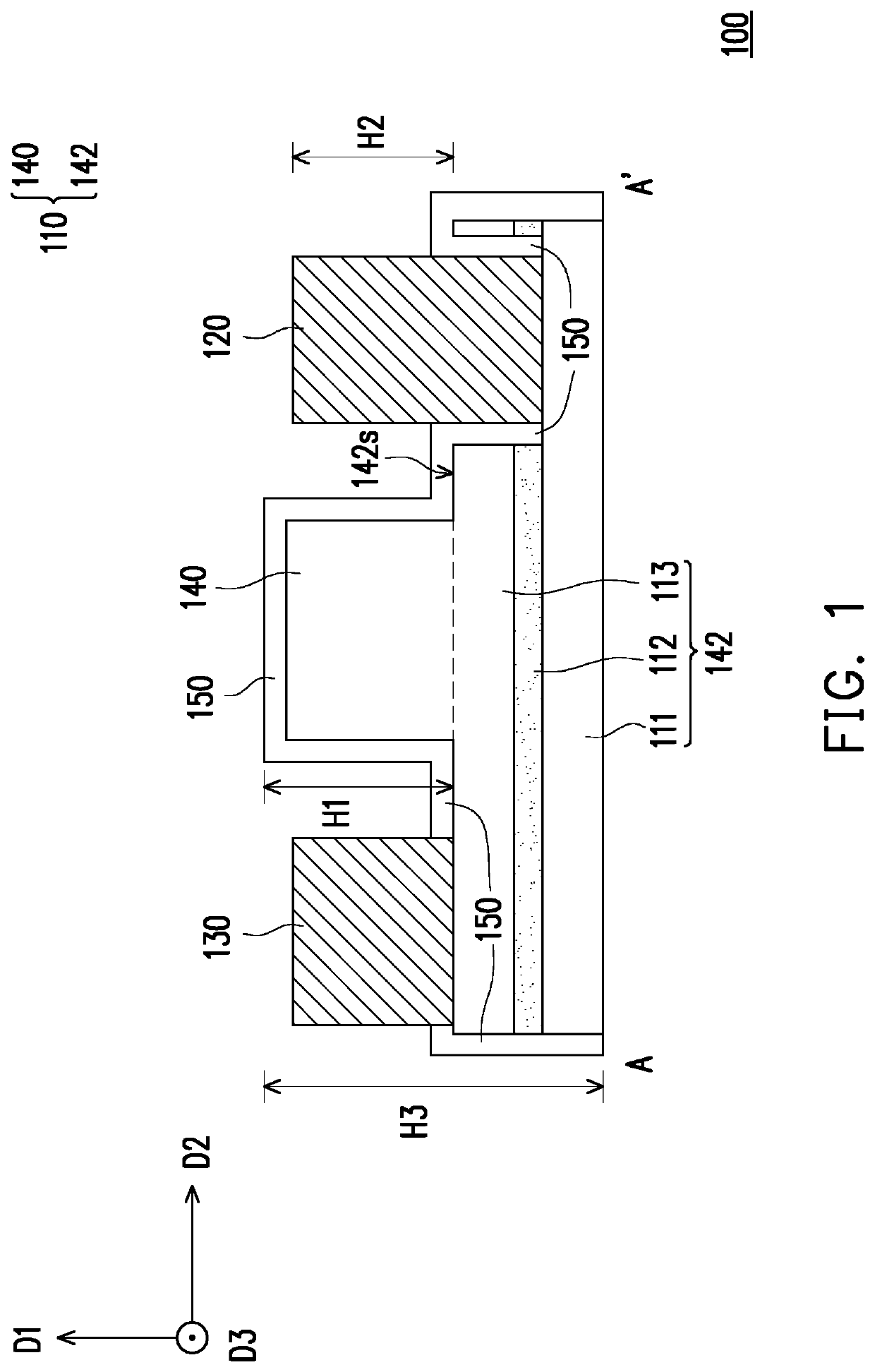
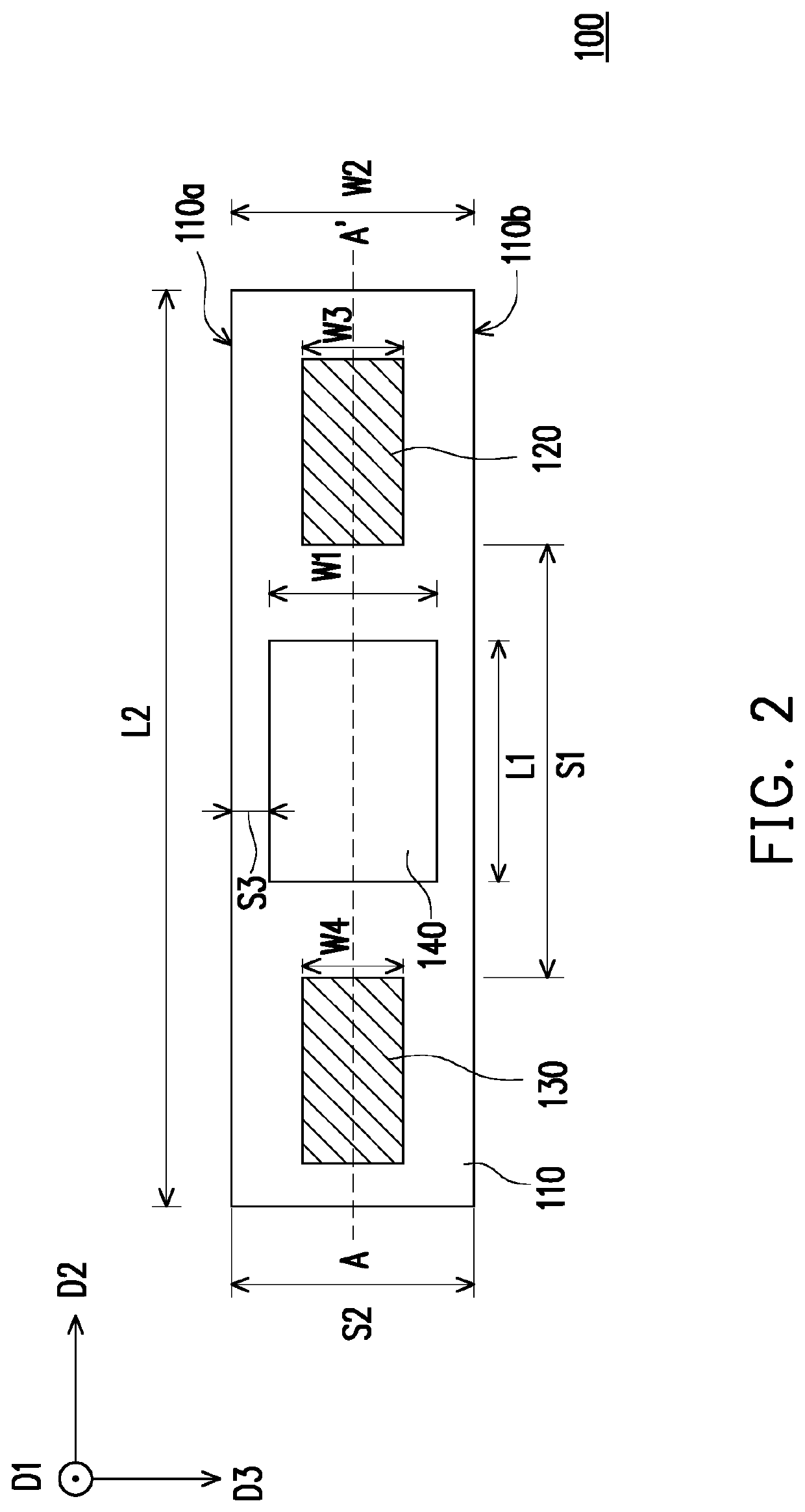
[0035]FIG. 1 is a schematic cross-sectional view of a micro light emitting device according to an embodiment of the invention. FIG. 2 is a schematic top view of a micro light emitting device according to an embodiment of the invention. FIG. 1 corresponds to a view taken along the line A-A′ of FIG. 2. It should be particularly noted that FIG. 2 omits the insulating layer 150 of FIG. 1.

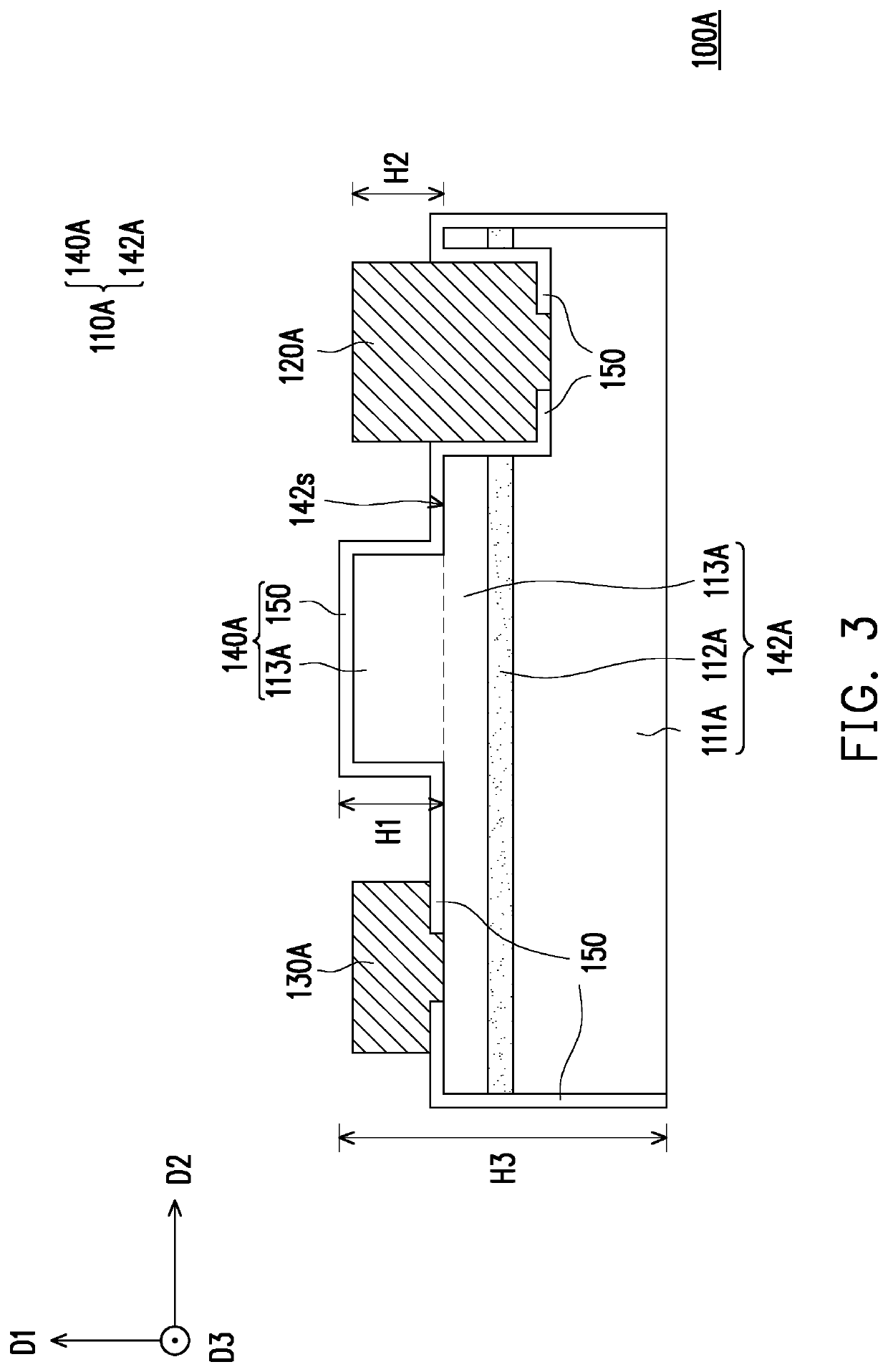
[0036]With reference to FIG. 1 and FIG. 2, in this embodiment, a micro light emitting device 100 includes a component layer 110, a first electrode 120 and a second electrode 130. The first electrode 120 is electrically connected to the component layer 110. The second electrode 130 is electrically connected to the component layer 110. The component layer 110 of the micro light emitting device 100 includes a protruding structure 140 and a main body 142. The protruding structure 140 is disposed between the first electrode 120 and the second electrode 130 and is disposed on the main body 142. The first elec...


PUM

PropertyMeasurementUnit
electrical propertiesaaaaaaaaaa
heightaaaaaaaaaa
lengthaaaaaaaaaa

Abstract

A micro light emitting device including a component layer, a first electrode and a second electrode is provided. The component layer includes a main body and a protruding structure disposed on the main body. The first electrode is electrically connected to the component layer. The second electrode is electrically connected to the component layer. The first electrode, the second electrode and the protruding structure are disposed on the same side of the main body. The protruding structure is located between the first electrode and the second electrode. A connection between the first electrode and the second electrode traverses the protruding structure. The main body has a surface. The protruding structure has a first height with respect to the surface. Any one of the first electrode and the second electrode has a second height with respect to the surface. The relation 0.8≤H1 / H2≤1.2 is satisfied, wherein H1 is the first height and H2 is the second height. A display apparatus having a plurality of micro light emitting devices is provided as well.

Description

CROSS-REFERENCE TO RELATED APPLICATION[0001]This application claims the priority benefit of Taiwan application serial no. 107125053, filed on Jul. 20, 2018. The entirety of the above-mentioned patent application is hereby incorporated by reference herein and made a part of this specification.BACKGROUND OF THE INVENTIONField of the Invention[0002]The invention relates to a light emitting device and a display apparatus, and particularly relates to a micro light emitting device and a display apparatus.Description of Related Art[0003]With the progress in optoelectronic technology, traditional incandescent bulbs and fluorescent lamps have been gradually replaced by a new generation of solid-state light sources such as light-emitting diodes (LEDs). The LEDs have advantages such as long-life span, miniature size, high vibration and shock resistance, high light efficiency and low power consumption, and thus have already been widely used as light sources in household lighting and various equ...

Claims


Application Information

Patent Timeline
Patent Type & Authority Patents(United States)
IPC IPC(8): H01L33/20H01L33/38H01L23/00H01L33/44H01L33/62H01L25/075H01L33/06H01L33/32
CPCH01L33/44H01L24/10H01L33/20H01L33/382H01L33/62H01L25/0753H01L33/06H01L33/32H01L2224/10145H01L24/16H01L33/644H01L2224/0401H01L2224/06102H01L2224/13109H01L2224/13111H01L2224/13144H01L2224/13147H01L2224/1403H01L2224/16238H01L2224/81193H01L2924/013H01L2924/00014
Inventor TSAI, PAI-YANGCHEN, FEI-HONGSHIH, YI-CHUN
Owner PLAYNITRIDE DISPLAY CO LTD
Learn More