Chip embedded substrate and method of producing the same

a technology of embedded substrates and chips, applied in the field of embedded substrates, can solve the problems of small substrate footprint, lower production efficiency, and lower production yield, and achieve the effect of high production yield and high reliability in electrical connection

Active Publication Date: 2011-08-02
SHINKO ELECTRIC IND CO LTD
View PDF34 Cites 61 Cited by
  • Summary
  • Abstract
  • Description
  • Claims
  • Application Information

AI Technical Summary

Benefits of technology

[0011]According to the present invention, a chip embedded substrate that enables high production yields and high reliability in electrical connection of the semiconductor chips to the multilayered wirings, and a production method of producing the same can be provided.

Problems solved by technology

In addition, high density mounting of the semiconductor chips onto a substrate, downsizing of the substrate on which the semiconductor chips are mounted, and a smaller footprint of the substrate are being required.
However, as the wiring structure of the chip embedded substrate becomes miniaturized and multilayered, it takes a longer time to produce the chip embedded substrate, which may bring about a disadvantage of lower production efficiency.
In addition, the miniaturized and multilayered wiring structure may cause lower production yields.
Especially, since expensive semiconductor chips are embedded in the chip embedded substrate, lower production yields of the chip embedded substrates may lead to a waste of many, expensive semiconductor chips.

Method used


Image

  • Chip embedded substrate and method of producing the same
  • Chip embedded substrate and method of producing the same
  • Chip embedded substrate and method of producing the same

Examples


example 1

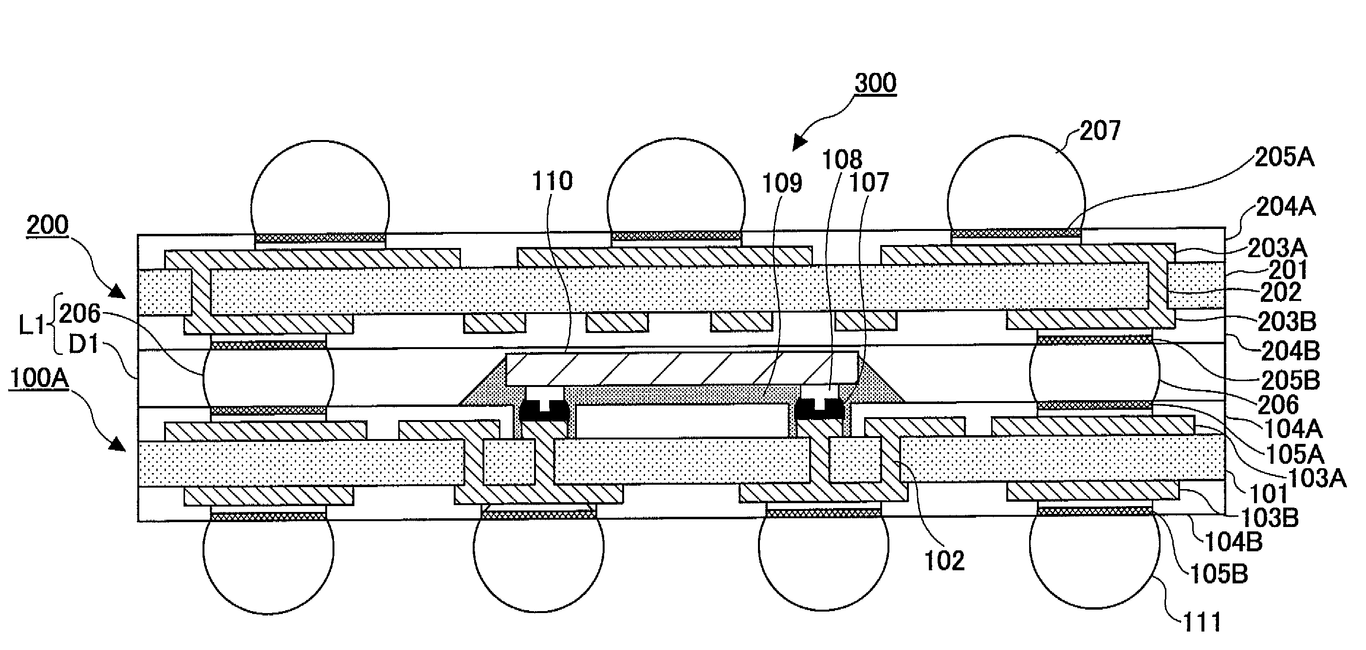
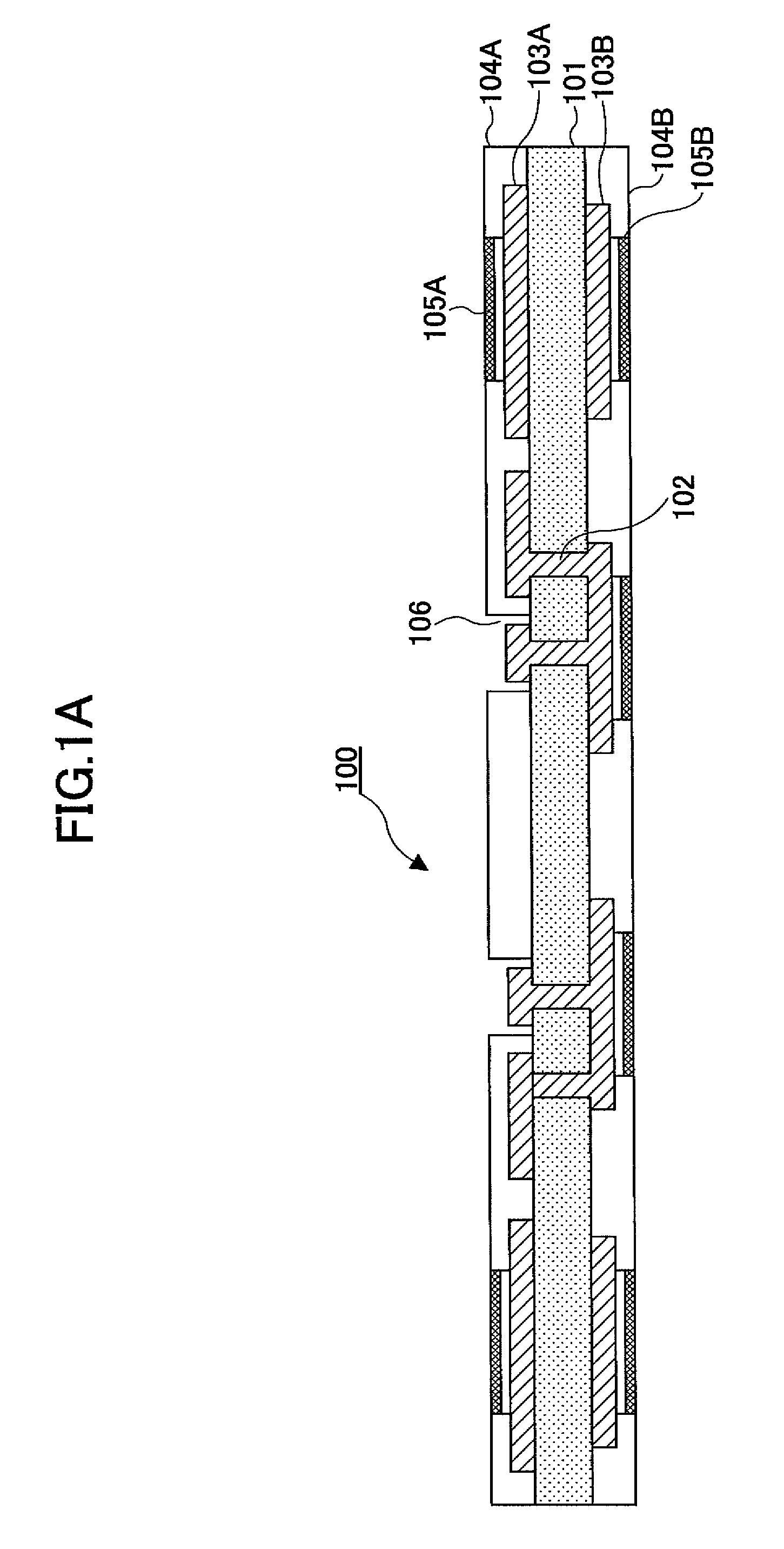
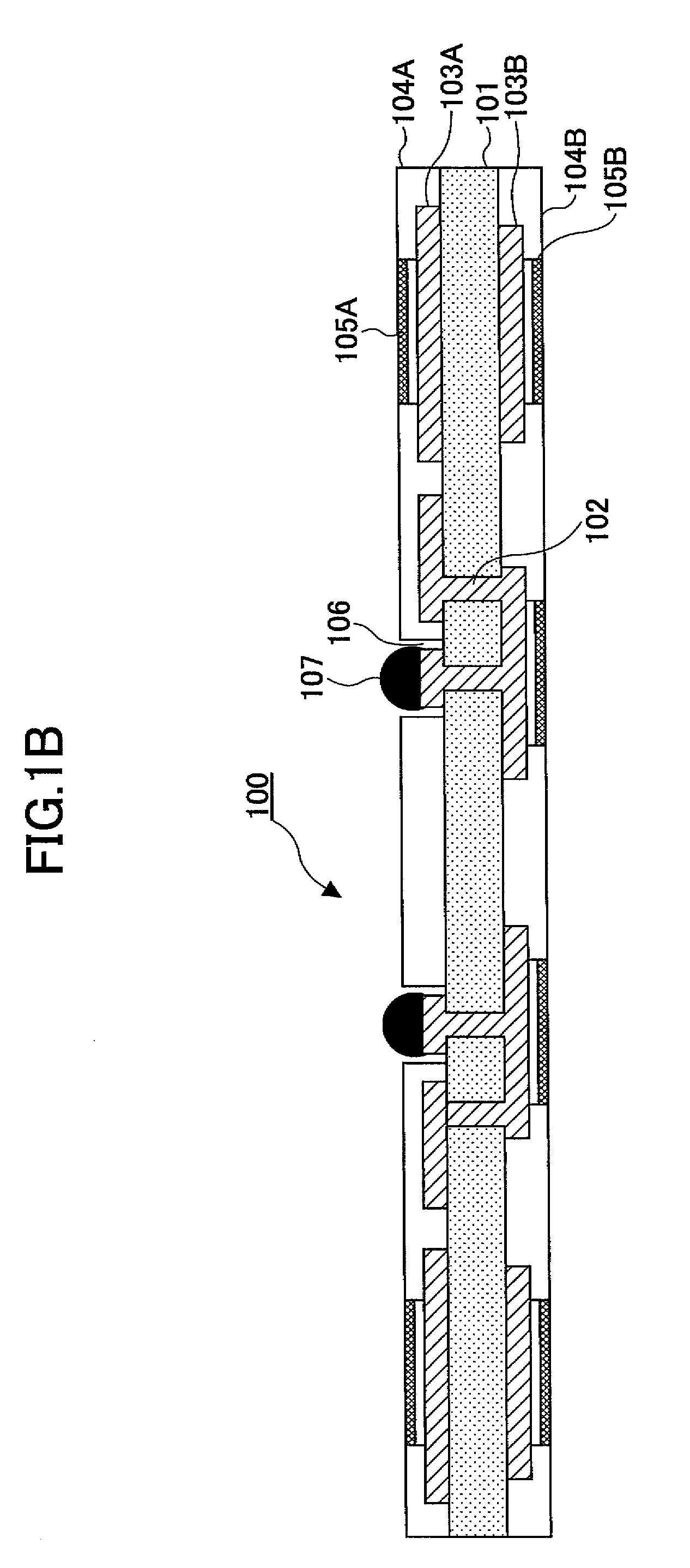
[0124]FIGS. 1A through 1F illustrate process steps of a production method of a chip embedded substrate according to a first example of the present invention. In the drawings, the same reference marks are given to portions described before and repetition of description may be eliminated.

[0125]In a process step shown in FIG. 1A, via plugs 102 formed of, for example, copper are made so as to pass through a core substrate 101 formed of, for example, a prepreg (a material made by impregnating epoxy resin or the like with fibrous glass). In addition, patterned wirings 103A are formed of, for example, copper on a first surface of the core substrate 101, and patterned wirings 103B are formed of, for example, copper on a second surface of the core substrate 101. On the first surface is mounted a semiconductor chip in a later process step.

[0126]Some of the patterned wirings 103A and the patterned wirings 103B are connected to each other through the via plugs 102.

[0127]On the first surface of ...

example 2

[0145]FIGS. 2A and 2B illustrate process steps of a production method of a chip embedded substrate according to a second example of the present invention.

[0146]First, process steps corresponding to the process steps of the first example shown in FIGS. 1A through 1D are carried out before arriving at a process step shown in FIG. 2A. However, in the process step corresponding to the process step shown in FIG. 1D, the solder balls 206 are not formed in the second example. Then, the process step shown in FIG. 2A, which corresponds to the process step shown in FIG. 1E, and the subsequent process steps are carried out.

[0147]Referring to FIG. 2A, an encapsulating connection layer L2, which corresponds to the encapsulating connection layer L1, is formed between the wiring substrate 200 and the wiring substrate 100A. The encapsulating connection layer L2 is formed of a connection layer D2 made of, for example, an anisotropic conductive material. As examples of the anisotropic conductive mate...

example 3

[0156]FIG. 3 illustrates an alteration of the chip embedded substrate 300 according to the first example. Referring to FIG. 3, a chip embedded substrate 300B according to the third example is obtained by stacking (joining) a wiring substrate 200A on the chip embedded substrate 300 after the process step shown in FIG. 1F of the first example.

[0157]The wiring substrate 200A is formed in the same manner as the wiring substrate 200. In this case, a core substrate 301, via plugs 302, patterned wirings 303A, 303B, solder resist layers 304A, 304B, connection layers 305A, 305B of the wiring substrate 200A correspond to the core substrate 201, the via plugs 202, the patterned wirings 203A, 203B, the solder resist layers 204A, 204B, and the connection layer 205A, 205B, respectively, and are made in the same manner using the same corresponding materials.

[0158]Above the solder resist layer 304A of the wiring substrate 200A, a semiconductor chip 307 and a semiconductor chip 309 are mounted. Spec...


PUM

PropertyMeasurementUnit
thicknessaaaaaaaaaa
electrically conductiveaaaaaaaaaa
electricalaaaaaaaaaa

Abstract

A method of producing a chip embedded substrate is disclosed. This method comprises a first step of mounting a semiconductor chip on a first substrate on which a first wiring is formed; and a second step of joining the first substrate with a second substrate on which a second wiring is formed. In the second step, the semiconductor chip is encapsulated between the first substrate and the second substrate and electrical connection is made between the first wiring and the second wiring so as to form multilayered wirings connected to the semiconductor chip.

Description

TECHNICAL FIELD[0001]The present invention relates to a chip embedded substrate having a semiconductor chip embedded.BACKGROUND ART[0002]Currently, electronic appliances using semiconductor devices, such as semiconductor chips, are highly sophisticated. In addition, high density mounting of the semiconductor chips onto a substrate, downsizing of the substrate on which the semiconductor chips are mounted, and a smaller footprint of the substrate are being required.[0003]In view of the above, a substrate in which the semiconductor chips are embedded, or a so-called chip embedded substrate, and various configurations for embedding the semiconductor chips in the substrate have been proposed. Additionally, along with progress in miniaturization of electric lines of the semiconductor chips, the wiring of the chip embedded substrate is also required to be miniaturized and multilayered.[0004]However, as the wiring structure of the chip embedded substrate becomes miniaturized and multilayere...

Claims


Application Information

Patent Timeline
Patent Type & Authority Patents(United States)
IPC IPC(8): H05K1/16
CPCH01L21/6835H01L23/552H01L24/81H01L24/97H01L25/105H01L25/162H05K1/186H01L24/83H01L25/16H05K1/185H01L21/56H01L21/563H01L21/565H01L23/3121H01L23/3128H01L23/49822H01L23/49833H01L23/5389H01L24/85H01L2221/68345H01L2224/1134H01L2224/13144H01L2224/16225H01L2224/16237H01L2224/32145H01L2224/48091H01L2224/48227H01L2224/73204H01L2224/73253H01L2224/73265H01L2224/81193H01L2224/81801H01L2224/83101H01L2224/83102H01L2224/83192H01L2224/92125H01L2224/97H01L2225/0651H01L2225/06568H01L2924/01002H01L2924/01004H01L2924/01015H01L2924/01027H01L2924/01029H01L2924/01033H01L2924/01075H01L2924/01078H01L2924/01079H01L2924/01082H01L2924/15311H01L2924/1532H01L2924/15331H01L2924/19041H01L2924/19042H01L2924/19043H01L2924/19104H01L2924/19105H01L2924/3025H05K3/20H05K3/4614H05K3/462H05K3/4644H05K2201/10378H05K2201/10674H01L2224/32225H01L24/48H01L2924/01005H01L2924/01006H01L2924/01019H01L2924/01087H01L2924/014H01L2224/85H01L2224/16145H01L2924/3511H01L2225/1023H01L2225/1041H01L2225/1058H01L2924/07811H05K2201/10007H05K2201/10977H01L2924/15192Y10T29/4913Y10T29/49144Y10T29/49146H01L2924/00014H01L2924/00H01L2924/00012H01L2224/81005H01L2924/181H01L2924/12042H01L24/73H01L2224/45144H01L24/45H01L2924/00011H01L2224/0401H01L2224/45015H01L2924/207H01L23/02H01L21/4853H01L21/4857H01L21/486H01L23/3114H01L23/5383H01L23/5384H01L23/5386
Inventor YAMANO, TAKAHARUIIZUKA, HAJIMESAKAGUCHI, HIDEAKIKOBAYASHI, TOSHIOARAI, TADASHIKOBAYASHI, TSUYOSHIKOYAMA, TETSUYAIIDA, KIYOAKIMASHIMA, TOMOAKITANAKA, KOICHIKUNIMOTO, YUJIYANAGISAWA, TAKASHI
Owner SHINKO ELECTRIC IND CO LTD
Why Eureka
Try Eureka