Substrate structure with embedded chip of semiconductor package and method for fabricating the same

a semiconductor package and embedded chip technology, applied in semiconductor devices, semiconductor/solid-state device details, electrical equipment, etc., can solve the problems of damage to the chip, high overall packaging cost, and inability to meet the requirements of electric performance, so as to improve the production yield of fabricating the carrier structure embedded with chips, and reduce the overall thickness of the semiconductor device.

Inactive Publication Date: 2006-04-27
PHOENIX PRECISION TECH CORP
View PDF11 Cites 64 Cited by
  • Summary
  • Abstract
  • Description
  • Claims
  • Application Information

AI Technical Summary

Benefits of technology

[0018] Referring to the substrate structure with embedded chips of a semiconductor package and the method for fabricating the same proposed in the present invention, at least a semiconductor chip is attached to a heat dissipating carrier structure by the means of a thermally conductive adhesive layer, such that heat generated by the semiconductor chip during operation can be effectively dissipated. Further, the semiconductor chip is embedded in the opening penetrating through the second carrier plate of the carrier structure, such that an overall thickness of the semiconductor device can be reduced to meet the requirement of miniaturization. Also, in the present invention, at least a build-up circuit structure is directly formed on the carrier structure embedded with the semiconductor chip, and the build-up circuit structure can be electrically connected to the conductive pad located on the semiconductor chip by the means of the conducive via. Moreover, the conductive elements such as solder balls, leads or metal bumps can be provided on the outer surface of the build-up circuit structure, such that the semiconductor package structure can be electrically connected to an external device. As the carrier structure of the present invention consists of two different materials such as two different metal layers, a flat integration surface can be formed in the second carrier plate using an etching or electroplating technique. Alternatively, the carrier structure can be consisted of a ceramic layer and a metal layer. An opening can be precast penetrating through the metal layer by the means of the ceramic layer or an opening can be precast penetrating through the ceramic layer by the means of

Problems solved by technology

If heat cannot be released immediately, the semiconductor package might be over heated to therefore damage the chip.
Recently, a ball grid array (BGA) structure is not able to satisfy the requirements of electric performances and heat dissipation when the number of leads exceeds 1500 pin and the frequency is over 5 GHz.
However, an overall packaging cost is very high and there are still many technique limitations.
Instead, other materials that cause unstable electrical, mechanical and physical properties are used.
Although the recess 104 for mounting the microelectronic

Method used


Image

  • Substrate structure with embedded chip of semiconductor package and method for fabricating the same
  • Substrate structure with embedded chip of semiconductor package and method for fabricating the same
  • Substrate structure with embedded chip of semiconductor package and method for fabricating the same

Examples


Embodiment Construction

[0029] The present invention is described in the following with specific embodiments, so that one skilled in the pertinent art can easily understand other advantages and effects of the present invention from the disclosure of the invention. The present invention may also be implemented and applied according to other embodiments, and the details may be modified based on different views and applications without departing from the spirit of the invention.

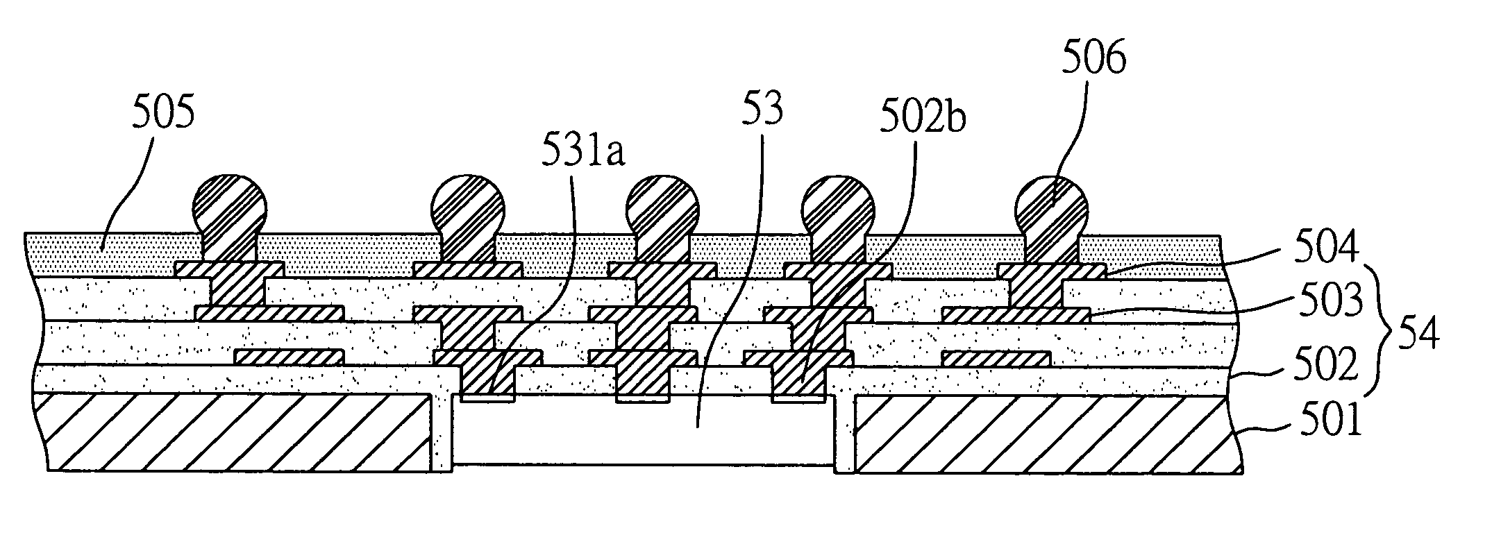
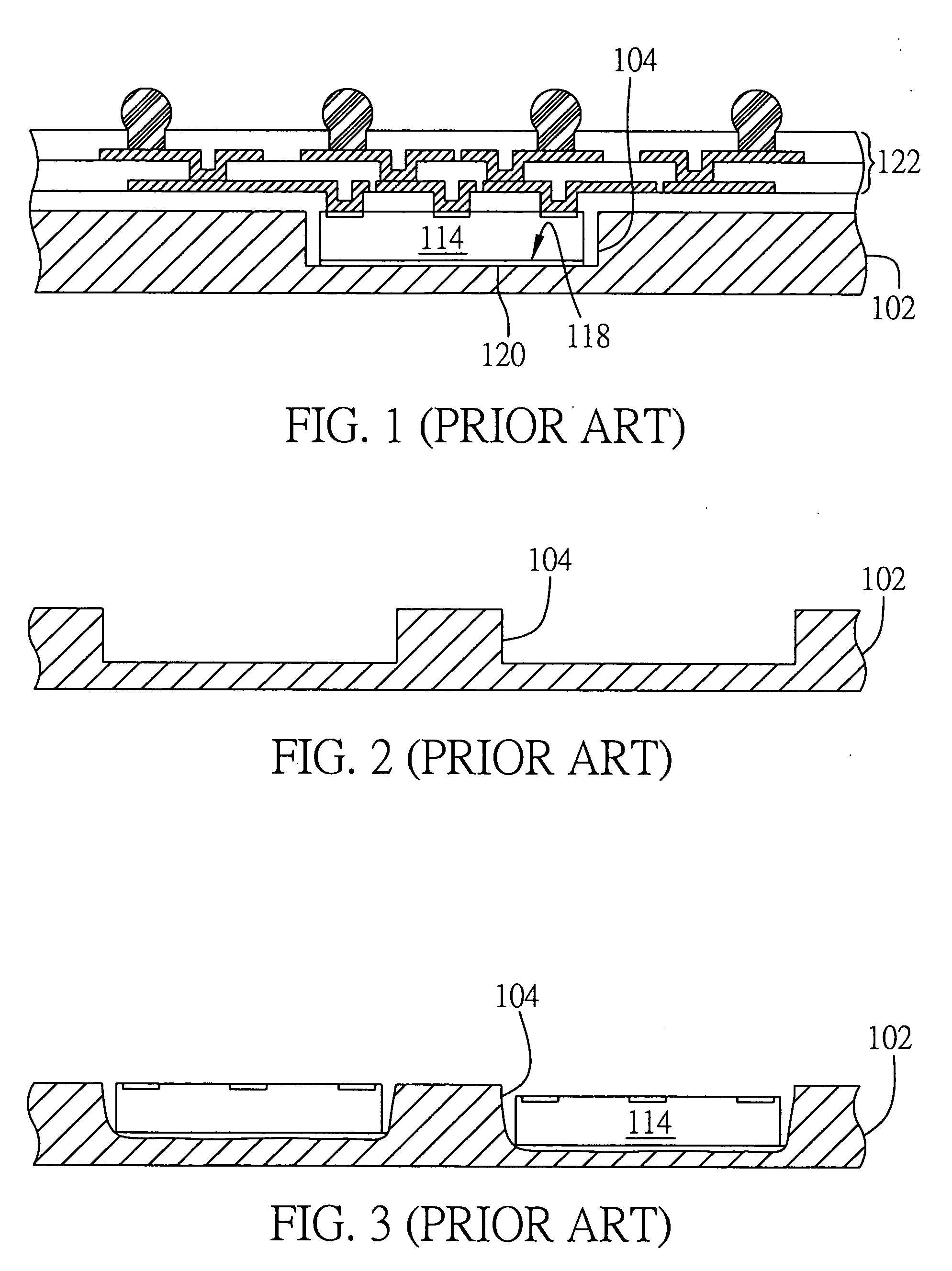
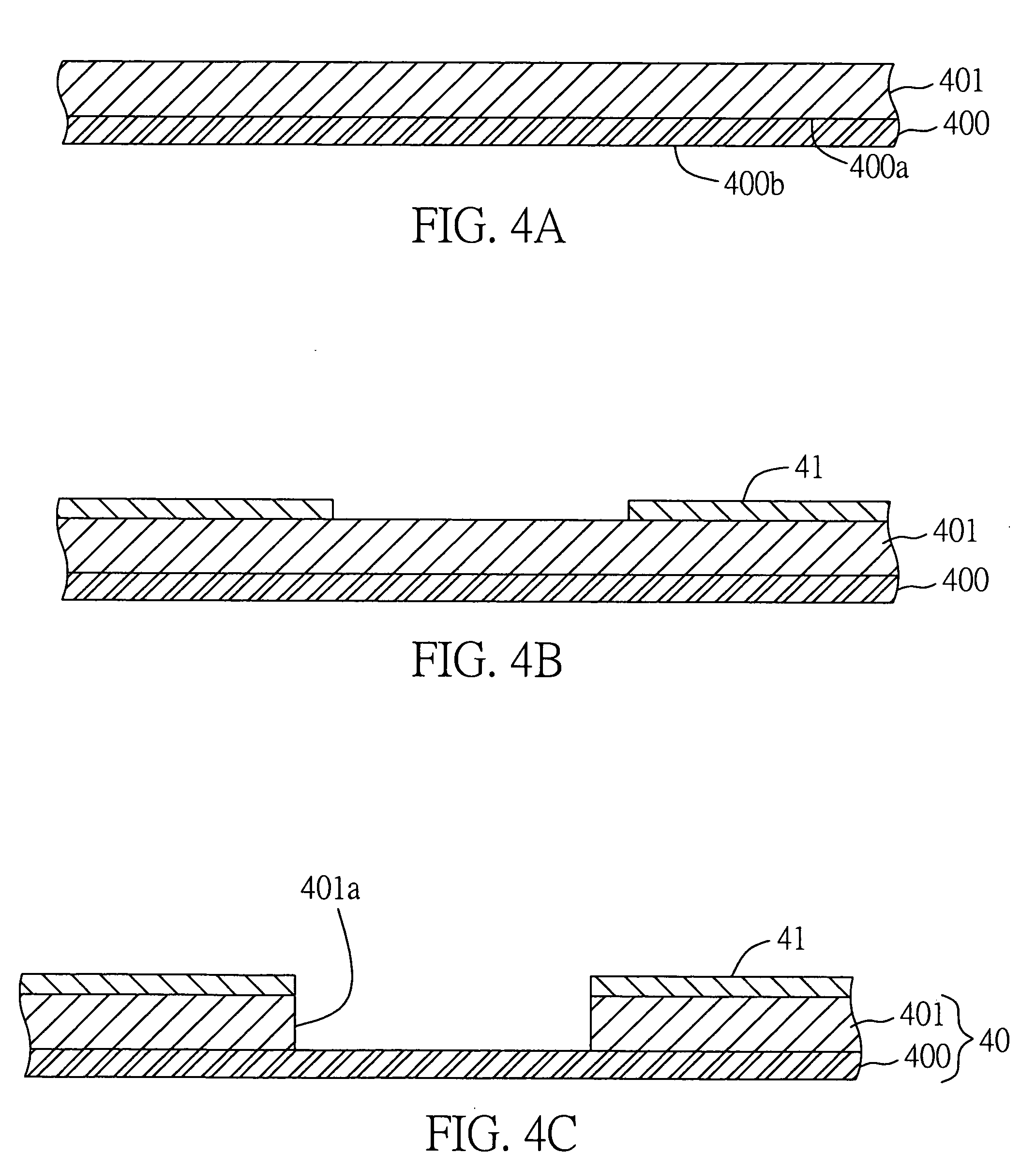
[0030] A preferred embodiment of a method for fabricating a substrate structure with embedded chips of a semiconductor package proposed in the present invention is described in detail with reference to FIG. 4A to FIG. 4J. What needs to be concerned here is that these drawings are simplified schematic diagrams, and thus only constructs relevant to the present invention are illustrated. Also, these constructs are not drawn according to actual amounts, shapes and dimensions. Actually, the amount, shape and dimension are an optional desig...


PUM


Abstract

A substrate structure with embedded chips of a semiconductor package and a method for fabricating the same are proposed. First of all, a carrier structure having a first carrier plate and a second carrier plate being directly formed on the first carrier plate is provided. The second carrier plate is provided with at least an opening. Then, a non-active surface of at least a semiconductor chip is mounted onto the first carrier plate and embedded in the opening of the second carrier plate. A dielectric layer is subsequently formed on a surface of the chip and the second carrier plate, and the material of the dielectric layer is filled in the opening of the second carrier plate. Afterwards, a plurality of vias is formed penetrating through the dielectric layer to expose conductive pads located on an active surface of the chip. A circuit layer and conductive vias are then respectively formed on a surface and penetrating through the dielectric layer, such that the circuit layer can be electrically connected to the conductive pad located on the chip by the means of the conductive via. Finally, conductive elements are provided on a surface of the circuit layer, so that the semiconductor chip embedded in the carrier plate can be electrically connected to an external device.

Description

FIELD OF THE INVENTION [0001] The present invention relates to a substrate structure with embedded chips of a semiconductor package and a method for fabricating the same, and more particularly, to a semiconductor package structure which integrates chips and carriers and a method for fabricating the same. BACKGROUND OF THE INVENTION [0002] Along with the blooming development of electronic industry, electronic products are gradually becoming more multi-functional and high efficient. In order to satisfy the requirements of high integration and miniaturization for semiconductor packages, a circuit board for carrying active / passive components and circuits is developed from a single-layer board into a multi-layer board, which is accomplished using the interlayer connection technique to enlarge usable area of the circuit board within limited space, so as to incorporate integrated circuits of high electronic density in the circuit board. [0003] However, as layers of conductive circuits and ...

Claims


Application Information

Patent Timeline
IPC IPC(8): H01L23/495H01L21/60H01L21/68H01L23/34H01L23/538
CPCH01L21/568H01L21/6835H01L23/5389H01L2224/24227H01L2224/82039H01L2924/14H01L2924/15153H01L2924/15165H01L2924/1517H01L2924/15174H01L2924/15311H01L2924/18162H01L2224/12105H01L2224/32245H01L2224/73267H01L24/19H01L2224/02379H01L2224/05001H01L2224/05008H01L2224/05024H01L2224/05026H01L2224/05548H01L2224/05569H01L2924/00014H01L2224/05599
Inventor HSU, SHIH-PING
Owner PHOENIX PRECISION TECH CORP
Why Eureka
Try Eureka