Novel bit line preparation method in MRAM fabrication

a technology of mram and line preparation, applied in the direction of basic electric elements, electrical apparatus, semiconductor devices, etc., can solve the problems of deterioration of magnetic performance, difficult control of the amount, and degradation of mtj performance, so as to improve the process window and reduce the mcb topography of the third embodiment.

Active Publication Date: 2011-04-21
TAIWAN SEMICON MFG CO LTD
View PDF10 Cites 62 Cited by
  • Summary
  • Abstract
  • Description
  • Claims
  • Application Information

AI Technical Summary

Benefits of technology

[0018]One objective of the present invention is to provide a MRAM structure that enables better control of the distance between a free layer in a MTJ and an overlying bit line or word line so that higher MRAM production yields are achieved and MRAM performance is enhanced.
[0019]A further objective of the present invention is to provide a method of forming the MRAM structure according to the first objective that is economical and reproducible on a manufacturing scale.
[0023]According to a third embodiment, a silicon nitride layer is deposited on the MCB layer prior to patterning and forming a plurality of MCBs. This method offers protection to the surface of the MCB layer during plasma etching, photoresist stripping, and wet cleaning steps. If the silicon nitride layer is sufficiently thick, then there is no need to deposit an extra silicon nitride layer for the dual damascene process.
[0024]A fourth embodiment is a modification of the third embodiment where a relatively thin silicon nitride layer is used to protect the MCB layer during the metal etch. In this case, a second silicon nitride layer is formed on the first silicon nitride layer and to fill the gaps between adjacent MCBs as part of the dual damascene process to form a bit line metal pattern. As a result, the large MCB topography of the third embodiment is considerably reduced to improve the process window during the dual damascene process.

Problems solved by technology

One of the challenges associated with MRAM fabrication is to control the distance between the free layer in a MTJ and an overlying conductive line such as BL 18 since the distance plays an important factor in determining the efficiency of switching the magnetization direction in the free layer during a write process.
Although this method is straightforward and can be successfully implemented for a MMC with a thick top electrode having a thickness greater than 200 Angstroms, there are several practical issues encountered for fabricating a MMC with a thin top electrode 17 (b-1f.
This design can easily lead to degradation in MTJ performance since the top electrode 17 is usually made of Ta and has a higher resistance than Cu in BL 18.
It is also difficult to control the amount of intrusion of top electrode into BL 18 and in some cases, the bit line may contact the free layer 16 to further deteriorate magnetic performance.
However, it is difficult to adjust the amount of overetch because one does not want to etch substantially beyond the top surface of top electrode 17 and risk forming a situation as described with regard to FIG. 1b.
However, this method teaches the formation of a top electrode separately from the magnetic memory cell which is generally not practiced in current designs where higher efficiency is achieved by forming the top electrode simultaneously with the magnetic memory cell.
This method does not prevent shorting or sub-trenches from forming especially when the capping layer (top electrode) is less than 200 Angstroms thick.
However, the invention does not provide a means to control subsequent etching processes from forming a sub-trench along the MTJ.
Although the additional thickness of the hard mask prevents bit line ILD etching from reaching the MTJ, it does add extra distance between MTJ and bit line and can therefore degrade free layer switching capability.

Method used


Image

  • Novel bit line preparation method in MRAM fabrication
  • Novel bit line preparation method in MRAM fabrication
  • Novel bit line preparation method in MRAM fabrication

Examples


first embodiment

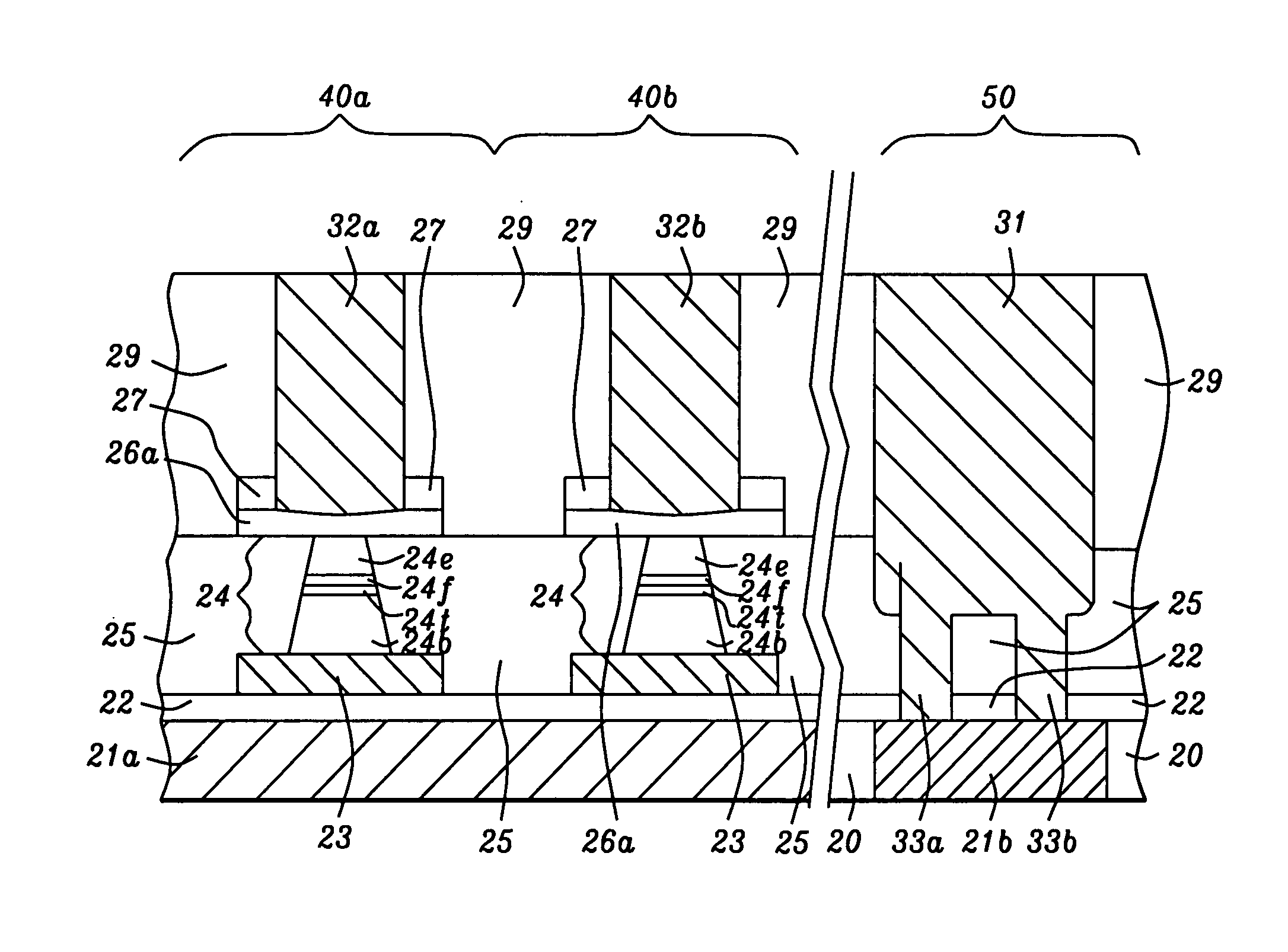
[0048] in FIG. 5, a wet cleaning process is performed to remove residues produced during the aforementioned metal plasma etch process. Since it is important to remove all metal residues to ensure that neighboring MCBs 26a are electrically isolated, the wet clean process may be applied for an extended period of time. Typically, due to the over etch and wet cleaning conditions, there is some erosion or etching of the top surface 25s of MTJ ILD layer 25 to form a new top surface 25t that is a distance d below the top surface of MCBs 26a. For a thin MCB 26a that is less than 100 Angstroms thick and with a certain amount of over etch and wet clean processing that causes less than 50 Angstroms loss of oxide (MTJ ILD 25), d which is also referred to as MCB depth or step height is typically less than 150 Angstroms and the resulting topography should not be severe enough to cause patterning issues for later process steps. With a MCB layer that is greater than 200 Angstroms thick and over etc...

fourth embodiment

[0059]the present invention represents a modification of the third embodiment. Referring to FIG. 8, a dielectric layer 27, preferably silicon nitride, is formed on the MCB layer 26 prior to fabricating a plurality of MCBs 26a. In this case, a thin silicon nitride layer preferably less than 100 Angstroms thick is used to reduce the step height after MCB patterning to less than d2 (not shown). Since the dielectric layer 27 that serves as a protective cap on MCBs 26a is relatively thin and may not be sufficiently thick to be an effective oxide etch stop layer, a second dielectric layer 28 which is preferably silicon nitride is deposited on dielectric layer 27 after the MCBs 26a are formed and a post-etch wet cleaning step is performed. Therefore, the total nitride thickness above MCBs 26a reaches a range of 200 to 500 Angstroms which is acceptable as an oxide etch stop layer during the trench forming step of a dual damascene process sequence. The BL ILD layer 29 (FIG. 14) may have a th...


PUM


Abstract

A MRAM structure is disclosed that includes a metal contact bridge (MCB) which provides an electrical connection between a MTJ top electrode and an overlying bit line. The MCB has a width greater than a MTJ top electrode and serves as an etch stop during bit line etching to prevent sub-trenches from forming adjacent to the top electrode and causing shorts. MCBs also prevent insufficient etching that causes open circuits. A MCB is preferably a metal, metal compound, or alloy such as Ta with low resistivity and high conductivity. The MCB layer is patterned prior to using a dual damascene process to form a bit line contacting each MCB and a bit line pad connection to a word line pad. MCB thickness is thin enough to allow a strong bit line magnetic field for switching a free layer and large enough to function as an efficient oxide etch stop.

Description

RELATED PATENT APPLICATION[0001]This application is related to the following: Docket # HMG09-047, Ser. No. ______, filing date ______; assigned to the same assignee as the current invention and which is herein incorporated by reference in its entirety.FIELD OF THE INVENTION[0002]The invention relates to an MRAM structure, and in particular, to a metal contact bridge (MCB) layer formed between a top surface of a magnetic tunnel junction (MTJ) and a bit line (BL) to control the MTJ-BL distance and avoid over etching and sub-trench formation that can lead to electrical shorting across the MTJ tunnel barrier layer.BACKGROUND OF THE INVENTION[0003]Magnetic random access memory (MRAM) that incorporates a MTJ as a magnetic memory storage cell (MMC) is a strong candidate to provide a high density and non-volatile storage solution for future memory applications. An MRAM array is generally comprised of an array of parallel first conductive lines on a horizontal plane, an array of parallel sec...

Claims


Application Information

Patent Timeline
Patent Type & Authority Applications(United States)
IPC IPC(8): H01L29/82H01L21/00
CPCH01L27/222H10B61/00
Inventor MAO, GUOMIN
Owner TAIWAN SEMICON MFG CO LTD
Why Eureka
Try Eureka