Semiconductor package having pre-plated leads and method of manufacturing the same

a technology of semiconductors and lead plates, which is applied in the direction of semiconductor devices, semiconductor/solid-state device details, electrical apparatus, etc., can solve the problems of delamination or mismatch of lead plates during the manufacture of packages, increase the cost, and thin, light devices, etc., and achieves good conductivity, high production yield, and easy access

Inactive Publication Date: 2007-01-18
ADVANCED SEMICON ENG INC
View PDF5 Cites 65 Cited by
  • Summary
  • Abstract
  • Description
  • Claims
  • Application Information

AI Technical Summary

Benefits of technology

[0009] It is therefore an object of the invention to provide a semiconductor package, particularly a QFN (Quad Flat Non-Lead) package, having pre-plated leads and method of manufacturing the same. With the pre-plated leads, the package havin

Problems solved by technology

One of the challenges is to provide the customers with a thin, light, but powerful device.
However, the conventional QFN package 10 as described above requires two-side half etching to configure the lead frame, so as to increase the cost of process.
Also, the thermal expansion coefficient of the die pad

Method used


Image

  • Semiconductor package having pre-plated leads and method of manufacturing the same
  • Semiconductor package having pre-plated leads and method of manufacturing the same
  • Semiconductor package having pre-plated leads and method of manufacturing the same

Examples


first embodiment

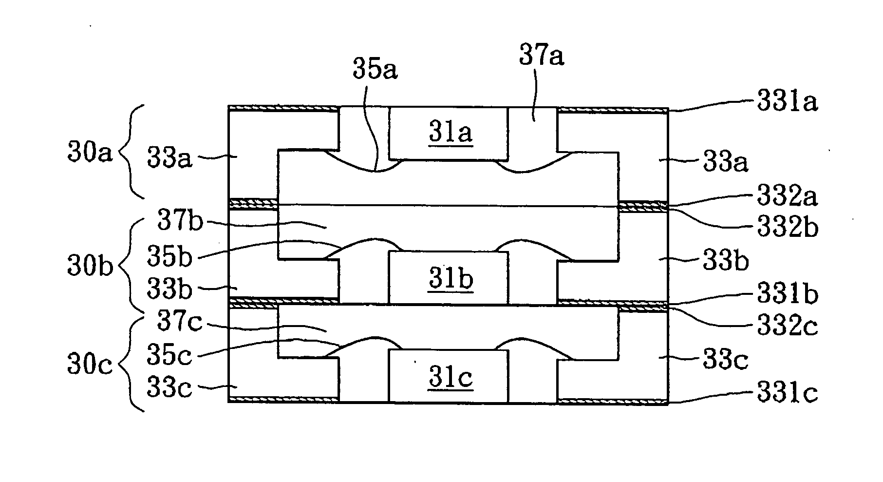
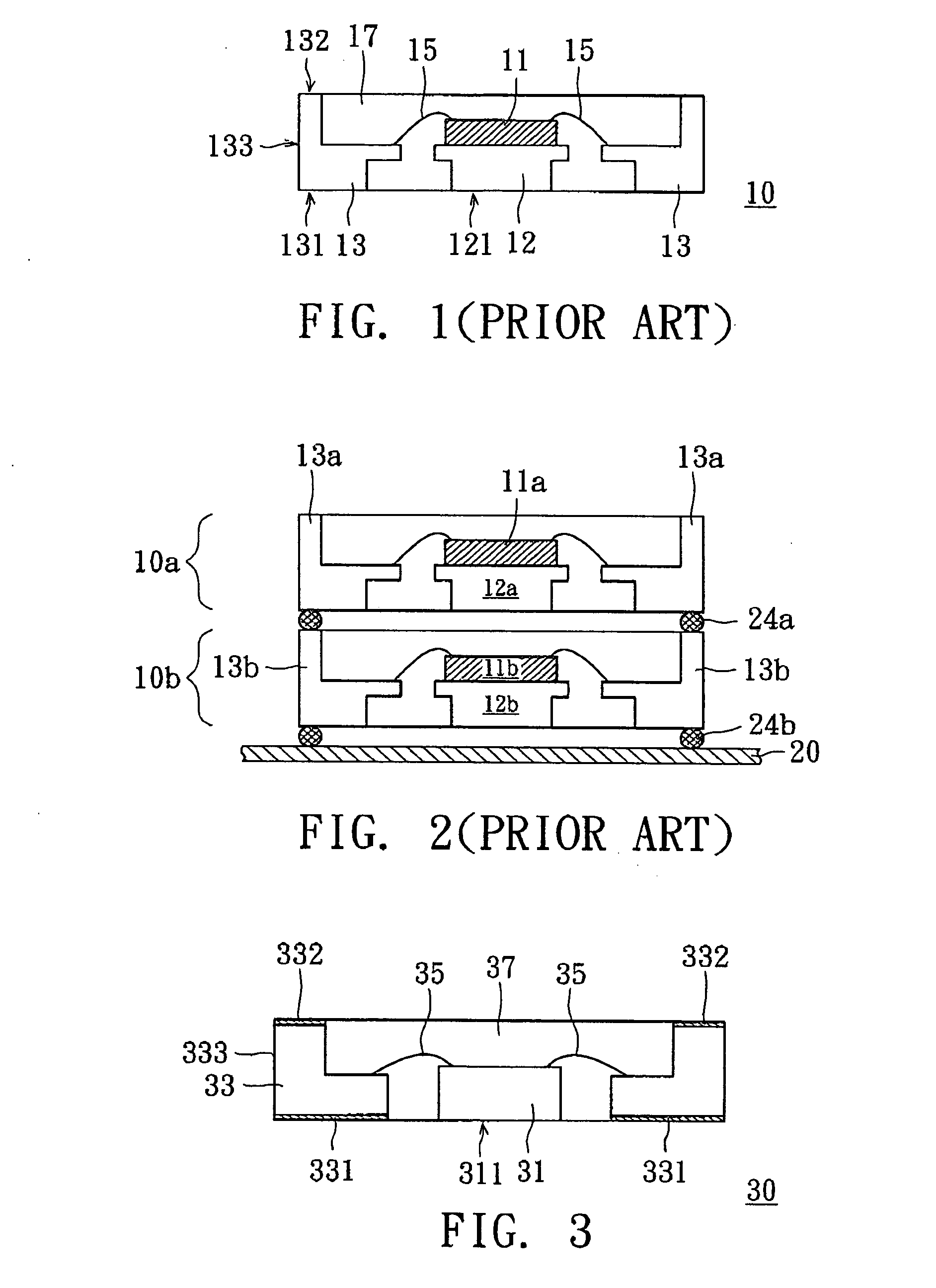
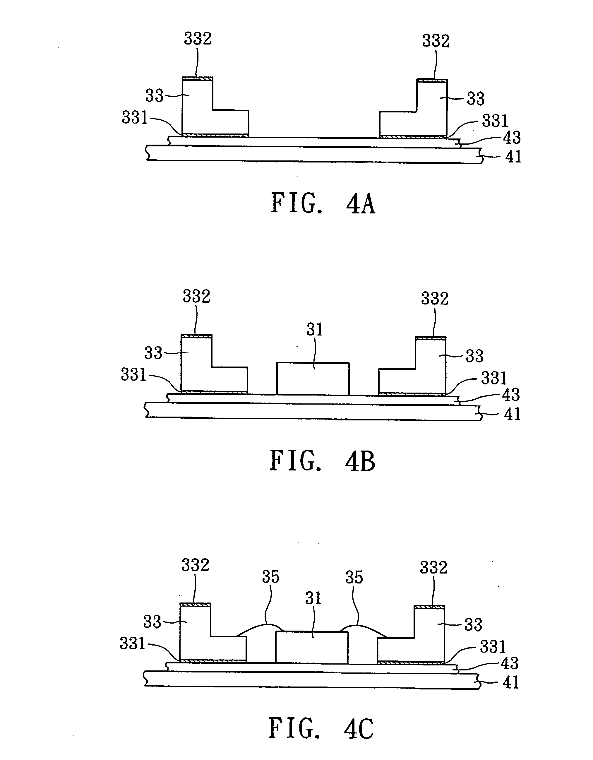
[0027]FIG. 3 is a cross-sectional view of a single QFN package according to the first embodiment of the invention. According to the first embodiment of the invention, the QFN package 20 comprises a die (i.e. semiconductor chip) 31, and a lead frame having the leads 33 surrounding the die 31. The lead frame, made of conductive material such as copper, copper alloy or iron-nickel alloy, is plated, so as to form the pre-plated conductive layers 331 and 332 respectively on the bottom portion and the top portion of the leads 33. The material of the pre-plated conductive layers 331 and 332 could be nickel (Ni), palladium (Pd), silver (Ag), or the alloy of the combination. Also, several bonding pads and bonding terminals (not shown) are formed on the die 31 and the leads 33, respectively. Each wire 35 connects the bonding pad of the die 31 and the bonding terminal of the lead 33 for the purpose of electrical connection of the die 31 and the lead 33. Also, a molding compound 37, made of a n...

second embodiment

[0033]FIG. 6 is a cross-sectional view of a single QFN package according to the second embodiment of the invention. The difference between the first (FIG. 3) and second (FIG. 6) embodiments is the die number applied in a single package. In the second embodiment, the QFN package 60 comprises a first die (i.e. mother chip) 61, a second die (i.e. daughter chip) 62 and a lead frame having the leads 63 surrounding the first die 61 and the second die 62. In the practical application, the first die 61 could be DDR, SRAM or Flash, and the second die 62 could be IPC, IPD or controller. According to the second embodiment, the second die 62 is attached to and electrically connected to the first die 61 through the conductive bumps 69 (such as the solder balls).

[0034] Also, the lead frame is plated to form the pre-plated conductive layers 631 and 632 respectively on the bottom portion and the top portion of the leads 63. The material of the pre-plated conductive layers 631 and 632 could be nick...

third embodiment

[0037]FIG. 8 is a cross-sectional view of a single QFN package according to the third embodiment of the invention. In the third embodiment, the QFN package 80 comprises a first die (i.e. mother chip) 81, a second die (i.e. daughter chip) 82 and a lead frame having the leads 83 surrounding the first die 81 and the second die 82. The difference between the second (FIG. 6) and third (FIG. 8) embodiments is the bonding method between the first die and the leads. According to the third embodiment, the first die 81 is electrically connected to the leads 83 through the first conductive bumps 86, and the second die 82 is electrically connected to the first die 81 through the second conductive bumps 89 (such as the solder balls).

[0038] Also, the lead frame is plated to form the pre-plated conductive layers 831 and 832 respectively on the bottom portion and the top portion of the leads 83. The material of the pre-plated conductive layers 631 and 632 could be nickel (Ni), palladium (Pd), silv...


PUM


Abstract

A quad flat non-lead (QFN) package at least comprises a die, a lead frame and a molding compound. The lead frame comprises a plurality of L-shaped leads for electrically connecting the die. Two pre-plated conductive layers, formed on a bottom portion and a top portion of each L-shaped lead, are exposed to a bottom surface and a top surface of the package, respectively. The molding compound is formed for encapsulating the die and the L-shaped leads.

Description

BACKGROUND OF THE INVENTION [0001] 1. Field of the Invention [0002] The invention relates in general to a semiconductor package having pre-plated leads and method of manufacturing the same, and more particularly to the QFN (Quad Flat Non-Lead) package having pre-plated leads and method of manufacturing the same. [0003] 2. Description of the Related Art [0004] In the recent years, the electronic devices, especially the portable products (e.g. digital mobile phone, digital camera and personal digital assistant), have been widely used. To meet the demand of the growing market, the semiconductor manufacturers face many challenges in supplying suitable electronic device of the electronic devices. One of the challenges is to provide the customers with a thin, light, but powerful device. Also, this device is much attractive if it is cost is much lower. Thus, a very thin, light and low-cost semiconductor package, so called as “Quad Flat Non-Lead” (QFN) package, has been developed to operate...

Claims


Application Information

Patent Timeline
IPC IPC(8): H01L23/495
CPCH01L21/568H01L2225/1041H01L23/3107H01L23/49548H01L23/49582H01L24/16H01L24/48H01L25/105H01L2224/16145H01L2224/32188H01L2224/48091H01L2224/48247H01L2924/01046H01L2924/01078H01L2924/15331H01L21/6835H01L2225/1029H01L2924/00014H01L2224/45099H01L2924/181H01L2924/18165H01L2224/16245H01L2924/18301H01L2924/00012
Inventor YANG, JUN-YOUNG
Owner ADVANCED SEMICON ENG INC
Why Eureka
Try Eureka