Radiation detecting apparatus, producing method therefor and radiation image pickup system
Inactive Publication Date: 2006-02-16
CANON KK
View PDF14 Cites 62 Cited by
Summary
Abstract
Description
Claims
Application Information
AI Technical Summary
This helps you quickly interpret patents by identifying the three key elements:
Problems solved by technology
Method used
Benefits of technology
Benefits of technology
[0011] According to the present invention, when a panel is set in an evaporation apparatus for forming the phosphor layer, it is so set that a holder portion constituting a masking portion is closely contacted with the frame member to execute a masking a non-forming area of the phosphor layer and a phosphor layer is deposited in this state. Such operation allows to form the phosphor layer under a masking of the connection lead and also to maintain a clearance between the connection lead on the sensor panel and the holder, thereby preventing the holder from approaching unexpectedly to the connection lead. It is thus rendered possible to prevent a discharge of the electrostatic charge accumulated on the sensor panel and to achieved a stable production with a high production yield.
[0012] Also the phosphor layer is covered by a frame member of a resin of a low moisture permeability in a lateral portion and by a phosphor protective layer provide on the upper surface, whereby a reliability against the moisturepermeation can be secured by a simple structure. Also the phosphor protective layer can be prepared within a short time in an inexpensive apparatus, by employing a hot-melt resin. Therefore a radiation detection apparatus of a low cost can be obtained.
Problems solved by technology
Also a masking may be achieved by covering the connection lead with a polyimide tape or the like before the setting in the phosphor forming apparatus, but there may result, when the masking tape is peeled off after the formation of the phosphor layer, a peeling charging of the sensor panel, thereby resulting in a discharge at a contact by the panel handling and causing similar failures.
Also in the aforementioned prior technology, the phosphor protective layer 113 and the protective layer 115 for reflective layer are formed by a CVD (gaseous growth) method requiring a vacuum evaporation apparatus, but such process necessitates an expensive apparatus and a very long forming time, leading to a high cost.
Method used
Image
Click on the blue label to locate the original text in one second.
Reading with bidirectional positioning of images and text.
Examples
example 1
[0047] In the following, an example 1 of the radiation detection apparatus of the invention will be explained in detail.
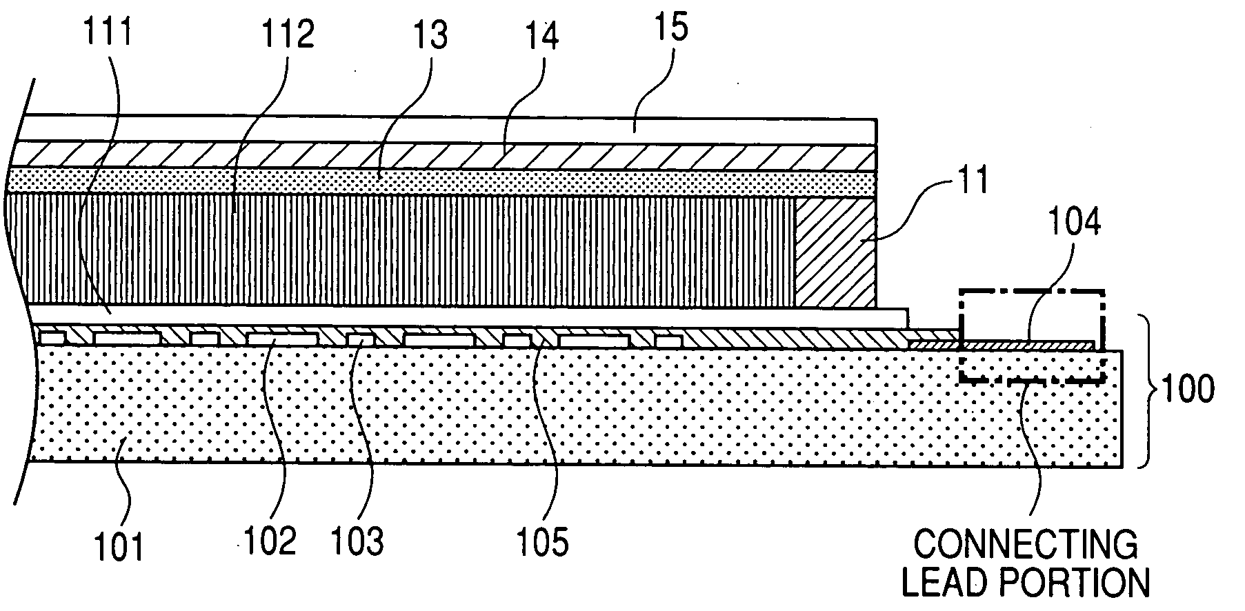
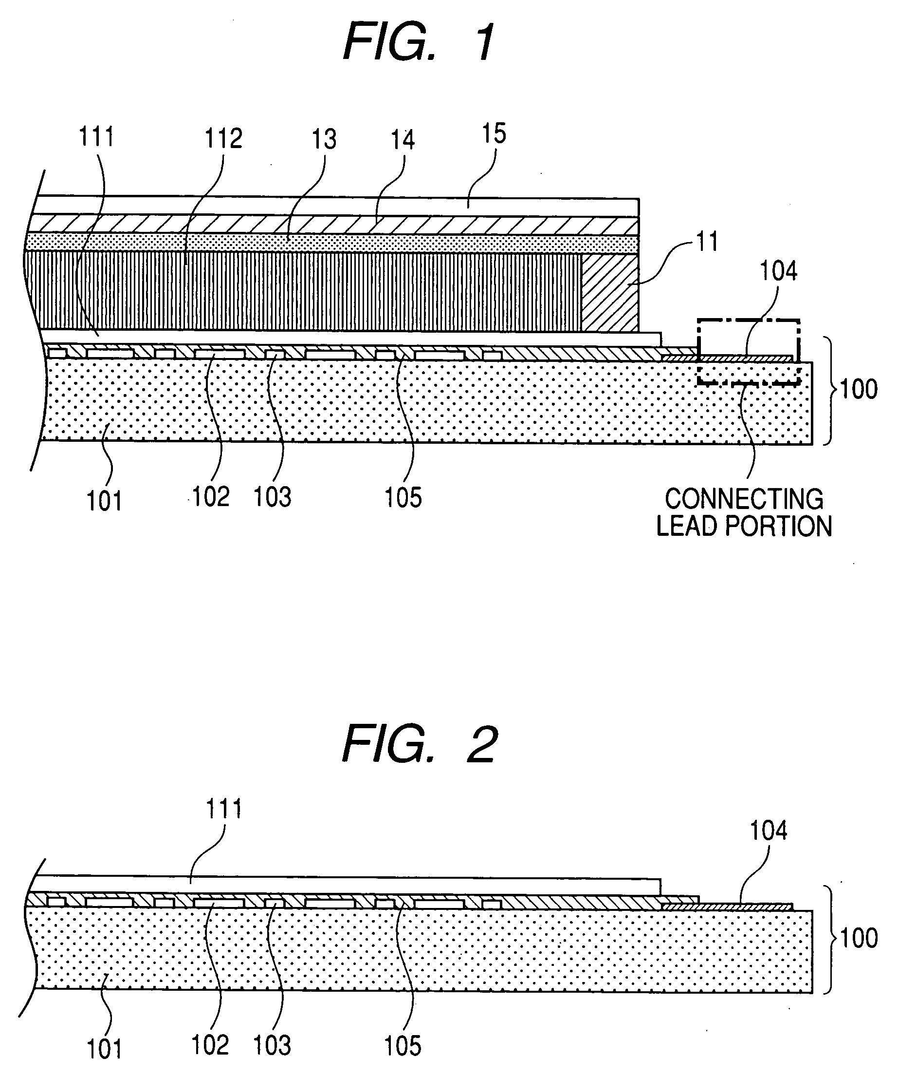
[0048] As shown in FIG. 2, on a semiconductor film of amorphous silicon prepared on a substrate 101 such as glass, there were prepared a photoelectric converting portion (photoreceiving unit) constituted of photosensors (photoelectric converting elements) and TFTs. A sensor panel 100 was prepared by forming thereon a sensor protective layer (first protective layer) 105 of SiNx and a phosphor undercoat layer 111 of cured polyimide resin.
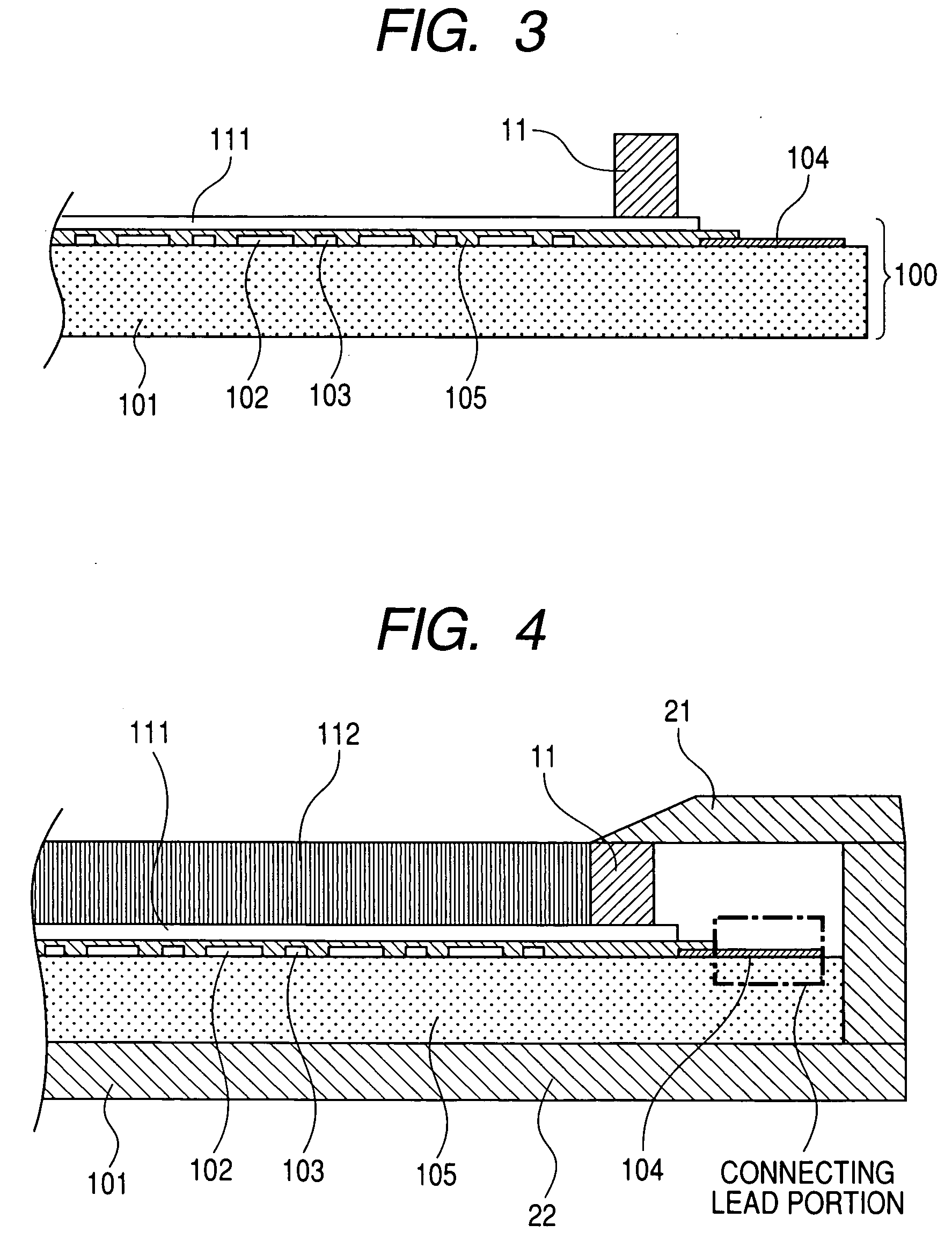
[0049] Then, as shown in FIG. 3, a frame member 11 of an epoxy resin was formed on the phosphor undercoat layer 111 in such a frame shape as to surround the two-dimensional photoelectric converting unit on the sensor panel, by coating with a dispensing apparatus with a width of 2 mm and a height of 0.5 mm, followed by curing. Then, as shown in FIG. 4, a phosphor layer 112 of an alkali halide phosphor of a columnar crystal structure...
example 2
[0052]FIG. 8 is a schematic partial cross-sectional view showing a radiation detection apparatus of example 2. Components same as or equivalent to those of the prior example shown in FIG. 11 and those of the example 1 in FIGS. 1, 2, 3 and 4 are indicated by same numbers and will not be explained repeatedly or only be briefly explained.
[0053] Also in the radiation detection apparatus shown in FIG. 8, as in the example 1, a frame member 11 was formed by a dispensing apparatus or a screen printing apparatus in such a frame shape as to surround the two-dimensional photoelectric converting unit. Thereafter a phosphor layer 112 was formed by placing a holder for vacuum evaporation, and a phosphor protective layer 13 was positioned and fixed so as to be in contact with the surface of the phosphor layer 112 and the frame member 11.
[0054] In the present example, as will be apparent from FIG. 8, the frame member 11 on the sensor panel 100 was so provided as to be in contact with both a phos...
example 3
[0055] In the examples 1 and 2, the frame 11 formed on the sensor panel was formed with a height same as that of the phosphor layer 112. However the present invention is not limited to such case, and the phosphor layer 112 may be formed with a height larger or smaller than that of the frame member 11.
[0056]FIG. 9 is a schematic partial cross-sectional view of a radiation detection apparatus of the example 3, showing an example in which the phosphor layer 112 was formed higher than the frame member 11.
[0057] In such case, when a phosphor protective layer 13 is formed by heat pressing with a heat roller as shown in FIG. 7A, the surface of the frame member 11 is positioned lower than the phosphor layer 112. Therefore, the pressure of the heat roller becomes weaker and a lower adhesion tends to result between the surface of the frame member 11 and the phosphor protective layer 13. Therefore, the adhesion was improved, as shown in FIG. 10, by thereafter executing a heat pressing (hot p...
PUM
Abstract
A radiation detection apparatus including a sensor panel, having a photoreceiving unit constituted of plural photoelectric converting elements two-dimensionally arranged on a substrate and electrical connecting portions provided in an external portion of the photoreceiving unit and electrically connected to the photoelectric converting elements of respective rows or columns of the photoreceiving unit, a phosphor layer provided at least on the photoreceiving unit for converting a radiation into a light detectable by the photoelectric converting element, and a phosphor protective member covering the phosphor layer and in contact with the sensor panel, characterized in that the phosphor protective member includes a frame member provided between the phosphor layer and the electric connecting portion on the sensor panel, and a phosphor protective layer covering an upper surface of the phosphor layer and provided in close contact with an upper surface of the frame member. This configuration allows to prevent a discharge of an electrostatic charge accumulated on the sensor panel, thereby providing a stable radiation detection apparatus with a high production yield.
Description
BACKGROUND OF THE INVENTION [0001] 1. Field of the Invention [0002] The present invention relates to a scintillator panel, a radiation detecting apparatus and a radiation image pickupsystem adapted for use in a medical diagnostic equipment or a non-destructive inspection equipment, and particularly to a scintillator panel, a radiation detecting apparatus and a radiation image pickupsystem adapted for use in an X-ray image pickup. In the present specification, the radiation includes also electromagnetic waves such as α-ray, β-ray or γ-ray in addition to X-ray. [0003] 2. Description of the Related Art [0004] For obtaining an X-ray photograph, there has been generally employed an X-ray film system including a fluorescent screen having an X-ray phosphor layer and an X-ray film coated on both sides. On the other hand, a digital radiation detection apparatus, including a phosphor layer as a wavelength converting member for converting an X-ray and a two-dimensional photodetector constitu...
Claims
Application Information
Patent Timeline
Application Date:The date an application was filed.
Publication Date:The date a patent or application was officially published.
First Publication Date:The earliest publication date of a patent with the same application number.
Issue Date:Publication date of the patent grant document.
PCT Entry Date:The Entry date of PCT National Phase.
Estimated Expiry Date:The statutory expiry date of a patent right according to the Patent Law, and it is the longest term of protection that the patent right can achieve without the termination of the patent right due to other reasons(Term extension factor has been taken into account ).
Invalid Date:Actual expiry date is based on effective date or publication date of legal transaction data of invalid patent.

