
Electro-optical device, manufacturing method for electro-optical device, and electronic apparatus

a manufacturing method and electrooptical technology, applied in the direction of electrical equipment, semiconductor devices, instruments, etc., can solve the problems of concave portion not being desirable, second insulating film formed inside the concave portion may peel off, etc., to achieve the effect of suppressing peeling

Active Publication Date: 2020-11-24
SEIKO EPSON CORP
View PDF5 Cites 2 Cited by
  • Summary
  • Abstract
  • Description
  • Claims
  • Application Information

AI Technical Summary

Benefits of technology

[0005]In light of the foregoing, an object of the invention is to provide an electro-optical device that, even when a concave portion resulting from a contact hole is leveled by an insulating film, is capable of suppressing peeling of the insulating film inside the concave portion, a manufacturing method for the electro-optical device, and an electronic apparatus.
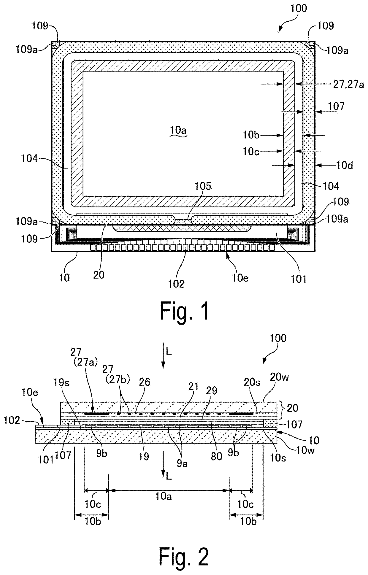
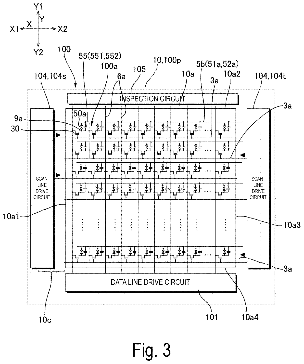
[0007]According to the aspect of the invention, the first electrode and the second electrode are electrically connected to each other via the first contact hole formed in the first insulating film, and at the same time, the surface of the second insulating film provided on the opposite side to the substrate with respect to the second electrode is leveled and the second electrode is exposed. Thus, leveling can be performed while filling the concave portion of the first contact hole using the second insulating film, and the pixel electrode can be provided on the flat surface configured by the second insulating film and the second electrode. As a result, the concave portion caused by the first contact hole can be prevented from occurring in the surface of the pixel electrode. Further, in the surface formed by the surface of the second electrode on the opposite side to the substrate and the surface of the first insulating film exposed from the second electrode, the second surface, which overlaps in a plan view with the second edge portion that is the part of the opening edge of the first contact hole, is on the substrate side with respect to the first surface, which overlaps in a plan view with the first edge portion that is the part of the opening edge of the first contact hole. Thus, in the second insulating film, the inside section positioned inside the concave portion overlapping in a plan view with the first contact hole is connected to the outside section overlapping with the second surface. As a result, peeling of the inside section can be suppressed after the leveling of the surface of the second insulating film on the opposite side to the substrate and before the formation of the pixel electrode.
[0011]According to the aspect of the invention, in a terminal region of the substrate, the electro-optical device may include a third electrode of the same layer as the first electrode, a second contact hole penetrating the first insulating film and the second insulating film at a position overlapping in a plan view with the third electrode, and a terminal provided on a surface of the second insulating film on the opposite side to the substrate and being electrically connected to the third electrode via the second contact hole. The pixel electrode may include a first electrically conducting film, and a second electrically conducting film provided on a surface of the first electrically conducting film on the opposite side to the substrate, and the terminal may be configured by an electrically conducting film of the same layer as the second electrically conducting film. According to this aspect, after the leveling of the surface of the second insulating film on the opposite side to the substrate, a process can be performed to form the second contact hole in a state in which the second insulating film is covered by the first electrically conducting film. Thus, the peeling of the inside section can be more effectively suppressed.
[0012]According to another aspect of the invention, an electro-optical device includes a substrate, a first electrode provided on a one surface side of the substrate, a first insulating film provided on a surface of the first electrode on an opposite side to the substrate, a first contact hole penetrating the first insulating film at a position overlapping in a plan view with the first electrode, a second electrode provided on a surface of the first insulating film on the opposite side to the substrate and being electrically connected to the first electrode via the first contact hole, a second insulating film provided with a surface configuring a flat surface continuous to a surface of the second electrode on the opposite side to the substrate, and a pixel electrode provided on a surface of the second insulating film on the opposite side to the substrate. In a terminal region of the substrate, the electro-optical device includes a third electrode of the same layer as the first electrode, a second contact hole penetrating the first insulating film and the second insulating film at a position overlapping in a plan view with the third electrode, and a terminal provided on a surface of the second insulating film on the opposite side to the substrate and being electrically connected to the third electrode via the second contact hole. Of the second insulating film, an inside section positioned inside a concave portion overlapping in a plan view with the first contact hole is separated from an outside section provided on the outside of the concave portion. The pixel electrode includes a first electrically conducting film, and a second electrically conducting film provided on a surface of the first electrically conducting film on the opposite side to the substrate, and the terminal is configured by an electrically conducting film of the same layer as the second electrically conducting film. According to this aspect, after the leveling of the surface of the second insulating film on the opposite side to the substrate, a process can be performed to form the second contact hole in a state in which the second insulating film is covered by the first electrically conducting film. Thus, the peeling of the inside section can be suppressed even when the inside section and the outside section of the second insulating film are separated from each other.

Problems solved by technology

This concave portion is not desirable as it may be a cause of disruption of the orientation of liquid crystal molecules in the liquid crystal device, for example.
Thus, after the leveling process, there is a risk that the second insulating film formed inside the concave portion may peel off before the forming of the pixel electrode.
For example, after the leveling process, and before the forming of the pixel electrode, when forming the contact hole, which reaches wiring formed on a lower layer side below the first insulating film, so as to penetrate the first insulating film and the second insulating film, after a resist mask is removed, when performing wet etching using hydrogen fluoride or the like in order to remove residue and the like remaining inside the contact hole, there is a risk that the second insulating film formed inside the concave portion may peel off.

Method used


Image

  • Electro-optical device, manufacturing method for electro-optical device, and electronic apparatus
  • Electro-optical device, manufacturing method for electro-optical device, and electronic apparatus
  • Electro-optical device, manufacturing method for electro-optical device, and electronic apparatus

Examples


exemplary embodiment 2

[0118

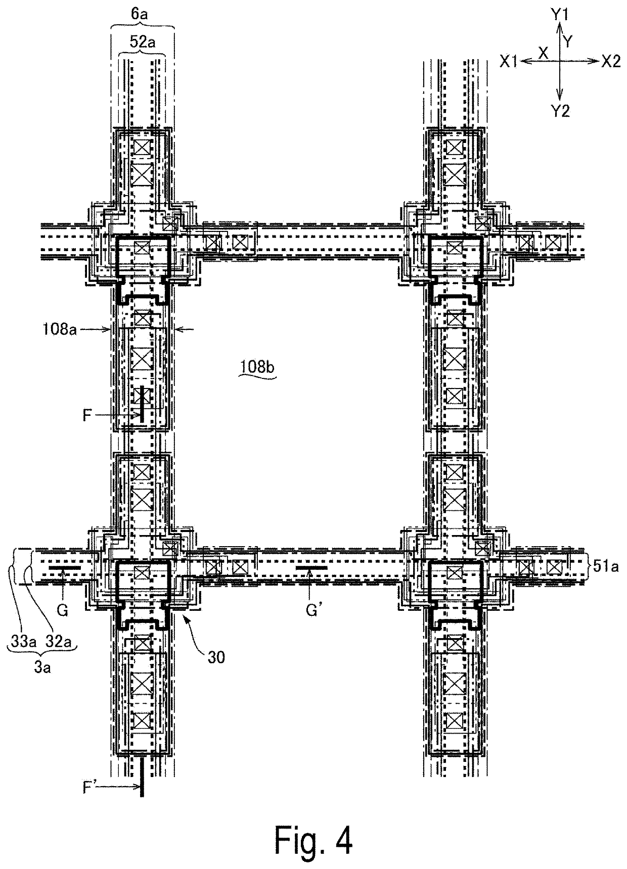
[0119]FIG. 17 is an explanatory diagram of the first substrate 10 used in the electro-optical device 100 according to Exemplary Embodiment 2 of the invention, and corresponds to the cross section G-G′ illustrated in FIG. 4. Note that basic configurations in this exemplary embodiment are the same as in Exemplary Embodiment 1, and thus, common portions are denoted by the same reference signs and a description of the common portions will be omitted. In Exemplary Embodiment 1, the first section 8a1 of the second electrode 8a is provided over both the first hole 17d6 and the second hole 17d7. In this exemplary embodiment, as illustrated in FIG. 17, on the first edge portion 17d1 side of the first contact hole 17d, the first section 8a1 is provided on both the first hole 17d6 and the second hole 17d7, but on the second edge portion 17d2 side, the first section 8a1 is provided only on the first hole 17d6 and is not provided on the second hole 17d7. The rest of the configuration is the...

exemplary embodiment 3

[0121

[0122]FIG. 18 is an explanatory diagram of the first substrate 10 used in the electro-optical device 100 according to Exemplary Embodiment 3 of the invention, and corresponds to the cross section G-G′ illustrated in FIG. 4. Note that basic configurations in this exemplary embodiment are the same as in Exemplary Embodiment 1, and thus, common portions are denoted by the same reference signs and a description of the common portions will be omitted. In Exemplary Embodiment 1, the first contact hole 17d includes the first hole 17d6 and the second hole 17d7 that is slightly larger than the first hole 17d6. In contrast, in this exemplary embodiment, as illustrated in FIG. 18, a section corresponding to the second hole 17d7 is formed so as to extend over a wide region on one side with respect to the first contact hole 17d, in addition to a region overlapping in a plan view with the first hole 17d6.

[0123]Thus, on the surface of the first insulating film 17 on the opposite side to the f...

exemplary embodiment 1

[0124]The second electrode 8a is provided with the first section 8a1 that is positioned inside the first contact hole 17d, and the second section 8a2 that extends from the first section 8a1 on the first step surface 17a on the outside of the first contact hole 17d while overlapping with the first edge portion 17d1. Furthermore, the second electrode 8a includes a third section 8a3 that extends from the first section 8a1 on the second step surface 17b on the outside of the first contact hole 17d while overlapping with the second edge portion 17d2. Here, the surface of the third section 8a3 on the opposite side to the first substrate 10 is positioned on the first substrate 10 side with respect to the surface of the second section 8a2 on the opposite side to the first substrate 10. Thus, the surface 170, which is formed by the surface of the second electrode 8a on the opposite side to the first substrate 10 and the surface of the first insulating film 17 exposed from the second electrod...


PUM

PropertyMeasurementUnit
thicknessaaaaaaaaaa
thicknessaaaaaaaaaa
sizeaaaaaaaaaa

Abstract

A first electrode, a first insulating film, a second electrode, a second insulating film, and a pixel electrode are formed on a one surface side of a first substrate of an electro-optical device. The second electrode is electrically connected [to the first electrode] via a first contact hole that penetrates the first insulating film. The second electrode and the second insulating film configure a continuous flat surface, which is the surface on the opposite side to the first substrate, and the pixel electrode is electrically connected to the second electrode. Of the second insulating film, since an inside section positioned inside a concave portion caused by the first contact hole is connected to an outside section provided on the outside of the concave portion, peeling of the inside section is unlikely to occur.

Description

BACKGROUND1. Technical Field[0001]The present invention relates to an electro-optical device provided with a pixel electrode on the opposite side of a substrate to an insulating film, a manufacturing method of the electro-optical device, and an electronic apparatus.2. Related Art[0002]In an electro-optical device, such as a liquid crystal device, an organic electroluminescence device and the like, since a relay electrode and an interlayer insulating film are connected in order between a substrate and a pixel electrode, in order to electrically connect the pixel electrode and the relay electrode, it is necessary to electrically connect the relay electrode and the pixel electrode via a contact hole formed in the interlayer insulating film. In this case, a concave portion caused by the contact hole occurs in the surface of the pixel electrode. This concave portion is not desirable as it may be a cause of disruption of the orientation of liquid crystal molecules in the liquid crystal de...

Claims


Application Information

Patent Timeline
Patent Type & Authority Patents(United States)
IPC IPC(8): G09G3/30H01L51/52H01L27/32G02F1/1333G02F1/1343G02F1/35
CPCH01L51/5203H01L27/3246H01L51/5253G02F1/133345G02F1/1343H01L27/3258H01L27/3248G02F2001/3505G02F1/136227G02F1/136213G02F2201/123G02F1/13439G02F2201/48H01L27/1248H01L27/124G02F1/133357G02F1/13629H10K59/123H10K59/124G02F1/3505H10K50/805H10K50/844H10K59/122
Inventor IIZUKA, SHOTAIZAWA, SHOTARO
Owner SEIKO EPSON CORP
Learn More