Method for quantification of process non uniformity using model-based metrology

a model-based metrology and process technology, applied in the field of semiconductor fabrication, can solve the problem that prior art systems are limited to a very specific set of analysis constraints

Active Publication Date: 2021-03-23
IBM CORP
View PDF83 Cites 0 Cited by
  • Summary
  • Abstract
  • Description
  • Claims
  • Application Information

AI Technical Summary

Problems solved by technology

This assumption leads to inaccuracies.
Furthermore, prior art systems are limited to a very specific set of analysis constraints.

Method used


Image

  • Method for quantification of process non uniformity using model-based metrology
  • Method for quantification of process non uniformity using model-based metrology
  • Method for quantification of process non uniformity using model-based metrology

Examples


Embodiment Construction

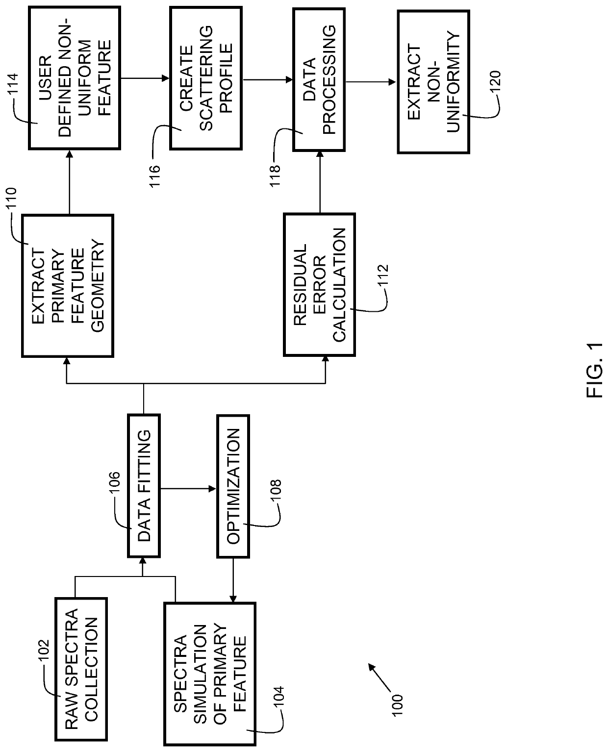
[0014]Embodiments of the present invention provide an improved method and system for assessing non-uniformity of features in the measurement area (within the beam spot) on a semiconductor structure, (e.g. wafer), such as a non-uniform film thickness. The scattering from non-uniform features is modeled. Post-processing the residual of theoretical and collected spectra is performed to assess a measure of non-uniformity from within an incident spot beam of a spectrum acquisition tool. Non-periodic topology differences have previously not been well accounted for in models. Embodiments of the present invention enable improved modeling for this type of manufacturing issue.

[0015]FIG. 1 is a flowchart 100 indicating process steps for embodiments of the present invention. In process step 102, raw (unprocessed) electromagnetic spectra are collected from physical samples. In embodiments, the raw spectra are acquired with a spectrum acquisition tool, such as a reflectometer tool or ellipsometer...


PUM

PropertyMeasurementUnit
diameteraaaaaaaaaa
diameteraaaaaaaaaa
diameteraaaaaaaaaa

Abstract

Embodiments of the present invention provide an improved method and system for assessing non-uniformity of features in the measurement area (within the beam spot) on a semiconductor structure, (e.g. wafer), such as a non-uniform film thickness. The scattering from non-uniform features is modeled. Post-processing the residual of theoretical and collected spectra is performed to assess a measure of non-uniformity from within an incident spot beam of a spectrum acquisition tool.

Description

FIELD OF THE INVENTION[0001]The present invention relates generally to semiconductor fabrication, and more particularly, to measurement of non-uniform features.BACKGROUND OF THE INVENTION[0002]Optical “scatterometry” attempts to evaluate the geometry of a sample based on the pattern of the diffracted light. More specifically, scatterometry systems use a modeling approach to transform scatterometry measurements into geometric measurements. For this type of approach, a theoretical model is defined for each physical structure that will be analyzed. The theoretical model predicts the empirical measurements (scatterometry signals) that scatterometry systems would record for the structure. The theoretical results of this calculation are then compared to the measured data. To the extent the results do not match, the theoretical model is modified and the theoretical data is calculated once again and compared to the empirical measurements. This process is repeated iteratively until the corre...

Claims


Application Information

Patent Timeline
Patent Type & Authority Patents(United States)
IPC IPC(8): G01N21/95G01B11/06G01N21/84G01N21/956
CPCG01N21/9501G01B11/0625G01B2210/56G01N21/8422G01N21/956G01N2021/8461
Inventor CHAO, ROBIN HSIN-KUOZHANG, YUNLIN
Owner IBM CORP
Why Eureka
Try Eureka