
Liquid crystal display device, driving method of the same, and electronic device including the same

a liquid crystal display and display device technology, applied in the direction of optics, digital storage, instruments, etc., can solve the problems of short circuit between the gate and the source or the drain of the transistor, and achieve the suppression of the characteristic deterioration of the pull-up transistor, the reduction of the channel width of the transistor, and the suppression of the characteristic deterioration of the transistor

Active Publication Date: 2021-03-30
SEMICON ENERGY LAB CO LTD
View PDF175 Cites 3 Cited by
  • Summary
  • Abstract
  • Description
  • Claims
  • Application Information

AI Technical Summary

Benefits of technology

The patent text describes a method for forming transistors using various substrates, such as semiconductor, single crystal, or plastic substrates. The use of different substrates can lead to variations in the characteristics of the transistor, such as size, current supply capability, and power consumption. However, by using a flexible substrate, such as paper or plastic, the transistor can be transferred to another substrate, which can improve its electrical characteristics, reduce power consumption, and improve reliability. The patent also suggests that circuits which are necessary for a desired function can be formed using one substrate, reducing the number of component parts and improving reliability. Additionally, the patent suggests that the layout area, size, and yield of a display device can be reduced, resulting in a high-definition display device or an increase in yield. The use of a flexible substrate can also reduce manufacturing costs and power consumption. Overall, the patent provides a method for improving the performance and efficiency of transistors in various applications.

Problems solved by technology

Alternatively, in some cases when the channel width of a transistor is large, a gate and a source or a drain of the transistor are likely to be short-circuited.

Method used


Image

  • Liquid crystal display device, driving method of the same, and electronic device including the same
  • Liquid crystal display device, driving method of the same, and electronic device including the same
  • Liquid crystal display device, driving method of the same, and electronic device including the same

Examples


embodiment 1

[0109]In this embodiment, one example of a semiconductor device will be described. The semiconductor device in this embodiment can be used for a variety of kinds of driver circuit, for example, a shift register, a gate driver, or a source driver. Note that the semiconductor device in this embodiment can also be referred to as a driver circuit or a circuit.

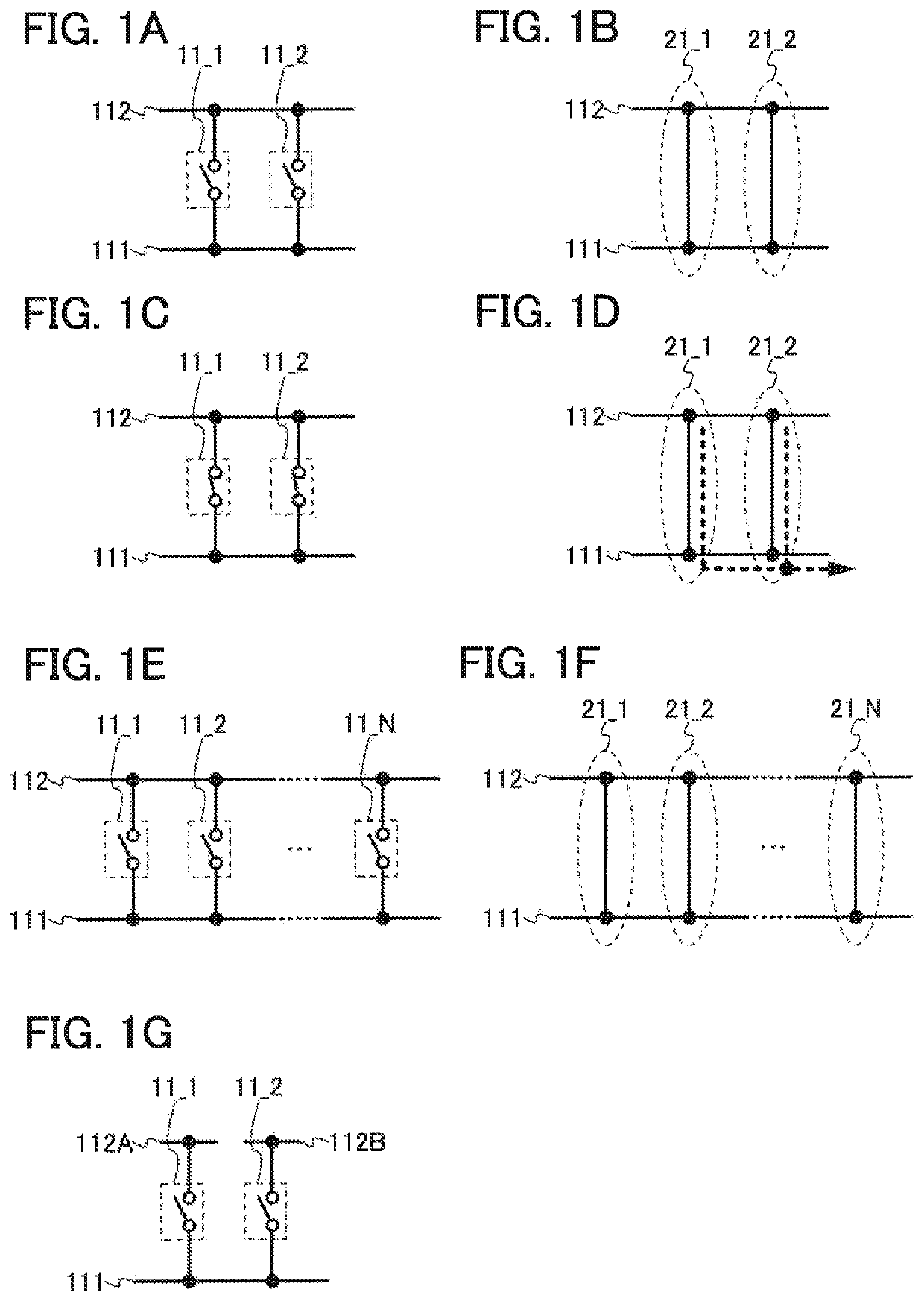
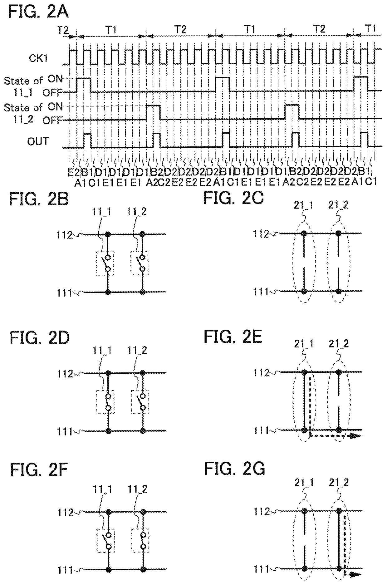
[0110]First, a semiconductor device of this embodiment will be described with reference to FIG. 1A. The semiconductor device in FIG. 1A includes a plurality of switches: switches 11_1 and 112. The switches 11_1 and 11_2 connects a wiring 111 and a wiring 112. However, this embodiment is not limited to this example. The semiconductor device can include three or more switches.

[0111]Next, an example of a signal, voltage, or the like which is input to or output from each wiring is described.

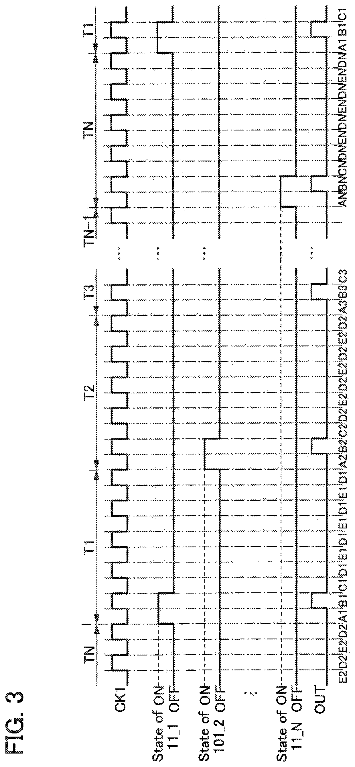
[0112]As an example, a signal OUT is output from the wiring 111. The signal OUT can have a first potential state and a second potential state, for ...

embodiment 2

[0151]In this embodiment, an example of a semiconductor device is described. The semiconductor device in this embodiment can include the semiconductor device described in Embodiment 1. Specifically, a structure in the case where, for example, a transistor is used as a switch included in the semiconductor device in Embodiment 1 is described. However, this embodiment is not limited to this example. A variety of elements, a variety of circuits, or the like can be used as a switch. Note that description of the content described in Embodiment 1 is omitted. Note that the content described in this embodiment can be combined with the content described in Embodiment 1 as appropriate.

[0152]First, the semiconductor device of this embodiment will be described with reference to FIG. 4A. The semiconductor device in FIG. 4 includes a circuit 100. The circuit 100 has a structure similar to that in the case where a transistor is used as a switch in the structure described in Embodiment 1. FIG. 4A sh...

embodiment 3

[0243]In this embodiment, an example of a structure which is different from that of the circuit 10 described in Embodiment 2 is described. Note that description of the content in Embodiments 1 and 2 is omitted. Note that the content described in this embodiment can be combined with the content described in Embodiments 1 and 2 as appropriate.

[0244]First, a specific example of the circuit 10 which is different from that in Embodiment 2 is described with reference to FIG. 14. The circuit 10 in FIG. 14 includes a circuit 300 in addition to the circuit 200. The circuit 300 is part of the circuit 10. Note that part of the circuit 300 can be used also as part of the circuit 200. Part of the circuit 200 can be used also as part of the circuit 300. The circuit 300 is connected to the wiring 113, the wiring 116, the wiring 117, the node n1, the node n2, and / or the wiring 111. However, this embodiment is not limited to this example. The circuit 200 can be connected to a variety of wirings or n...


PUM

PropertyMeasurementUnit
threshold voltageaaaaaaaaaa
clock frequencyaaaaaaaaaa
capacitanceaaaaaaaaaa

Abstract

It is an object to suppress deterioration of characteristics of a transistor in a driver circuit. A first switch for controlling whether to set a potential state of an output signal by being turned on and off in accordance with the first input signal, and a second switch for controlling whether to set a potential state of an output signal by being turned on and off in accordance with the second input signal are included. A first wiring and a second wiring are brought into electrical continuity by turning on and off of the first switch or the second switch.

Description

CROSS-REFERENCE TO RELATED APPLICATIONS[0001]This application is a continuation of U.S. application Ser. No. 12 / 731,203, filed Mar. 25, 2010, now pending, which claims the benefit of a foreign priority application filed in Japan as Serial No. 2009-077200 on Mar. 26, 2009, both of which are incorporated by reference.BACKGROUND OF THE INVENTION1. Field of the Invention[0002]The present invention relates to a semiconductor device, a display device, a liquid crystal display device, a method for driving these devices, and a method for manufacturing these devices. The present invention particularly relates to a semiconductor device, a display device, and a liquid crystal display device which include driver circuits formed over the same substrates as pixel portions, and a method for driving these devices. Further, the present invention relates to an electronic device including the semiconductor device, the display device, or the liquid crystal display device.2. Description of the Related A...

Claims


Application Information

Patent Timeline
Patent Type & Authority Patents(United States)
IPC IPC(8): G11C19/18G02F1/1362G11C19/28G09G3/34G02F1/1335G09G3/36
CPCG09G3/3677G09G3/3688G11C19/28G09G2300/0417G09G2310/0286G09G2320/043G09G3/3266G09G2310/0267G09G2330/021
Inventor KIMURA, HAJIMEUMEZAKI, ATSUSHI
Owner SEMICON ENERGY LAB CO LTD
Learn More