

Semiconductor device, display panel, method for manufacturing semiconductor device, method for manufacturing display panel, and information processing device
a technology for semiconductor devices and display panels, which is applied in the direction of semiconductor devices, organic semiconductor devices, semiconductor devices, etc., to achieve the effects of high convenience or reliability, and high convenience or reliability
- Summary
- Abstract
- Description
- Claims
- Application Information
AI Technical Summary
Benefits of technology
Problems solved by technology
Method used
Image

Examples
embodiment 1
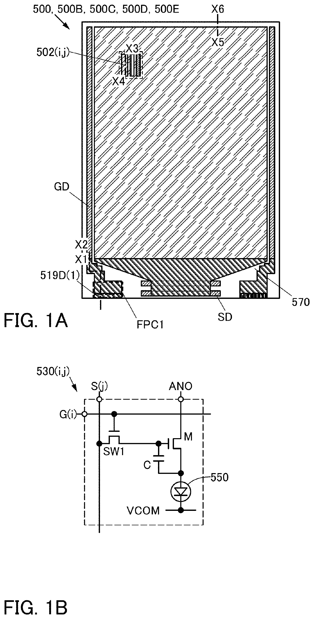
[0085]In this embodiment, the structure of a semiconductor device of one embodiment of the present invention will be described with reference to FIGS. 1A and 1B and FIGS. 2A to 2C.
[0086]FIGS. 1A and 1B illustrate the structure of a semiconductor device of one embodiment of the present invention. FIG. 1A is a top view of a semiconductor device 500 of one embodiment of the present invention, and FIG. 1B is a circuit diagram of a circuit which can be used for the semiconductor device 500.
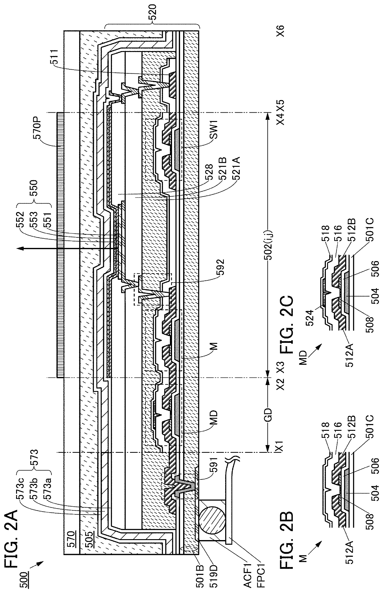
[0087]FIGS. 2A to 2C illustrate the structure of the semiconductor device 500 of one embodiment of the present invention. FIG. 2A is a cross-sectional view of the semiconductor device 500 taken along the section lines X1-X2, X3-X4, and X5-X6 in FIG. 1A. FIG. 2B is a cross-sectional view illustrating the details of a transistor M in FIG. 2A, and FIG. 2C is a cross-sectional view illustrating the details of a transistor MD in FIG. 2A. Note that in this specification, an integral variable of 1 or more may...
embodiment 2
[0306]In this embodiment, a method for manufacturing a semiconductor device of one embodiment of the present invention will be described with reference to FIG. 5, FIGS. 6A1 to 6D2, and FIGS. 7A1 to 7D2.
[0307]FIG. 5 is a flow chart showing the method for manufacturing a semiconductor device of one embodiment of the present invention. FIGS. 6A1 to 6D2 and FIGS. 7A1 to 7D2 illustrate the method for manufacturing a semiconductor device of one embodiment of the present invention.
[0308]FIGS. 6A2, 6B2, 6C2, and 6D2 are each a top view of members during the manufacturing process of the semiconductor device. FIG. 6A1 is a cross-sectional view taken along the section line W1-W2 in FIG. 6A2. FIG. 6B1 is a cross-sectional view taken along the section line W1-W2 in FIG. 6B2. FIG. 6C1 is a cross-sectional view taken along the section line W1-W2 in FIG. 6C2. FIG. 6D1 is a cross-sectional view taken along the section line W1-W2 in FIG. 6D2.
[0309]FIGS. 7A2, 7C2, and 7D2 are each a top view of member...
embodiment 3
[0336]In this embodiment, a method for manufacturing a semiconductor device of one embodiment of the present invention will be described with reference to FIG. 8, FIG. 9, FIG. 10, FIG. 11, FIG. 12, FIG. 13, and FIG. 14.
[0337]FIG. 8 is a flow chart showing the method for manufacturing a semiconductor device of one embodiment of the present invention. FIG. 9, FIG. 10, FIG. 11, FIG. 12, FIG. 13, and FIG. 14 illustrate the method for manufacturing a semiconductor device of one embodiment of the present invention.
[0338]FIG. 9, FIG. 10, FIG. 11, FIG. 12, FIG. 13, and FIG. 14 are cross-sectional views of members during the manufacturing process of the semiconductor device 500 taken along the section lines X1-X2, X3-X4, and X5-X6 in FIG. 1A.
[0339]A method for manufacturing a semiconductor device described in this embodiment includes the following nine steps (see FIG. 8).
[0340]The semiconductor device 500 described in this embodiment includes the second insulating film 501B having an opening...
PUM
| Property | Measurement | Unit |
|---|---|---|
| thickness | aaaaa | aaaaa |
| thickness | aaaaa | aaaaa |
| sizes | aaaaa | aaaaa |
Abstract
Description
Claims
Application Information