Stack of electrical components and method of producing the same

a technology of electrical components and conductive layers, which is applied in the direction of electrical apparatus, semiconductor devices, semiconductor/solid-state device details, etc., can solve the problems of deteriorating electrical reliability of the conductive layer, and achieve the reduction of the required distance between the pad the first electrical component, and the limitation of the downsizing of the second electrical component can be mitigated.

Active Publication Date: 2021-08-10
TDK CORPARATION
View PDF13 Cites 1 Cited by
  • Summary
  • Abstract
  • Description
  • Claims
  • Application Information

AI Technical Summary

Benefits of technology

[0004]Generally, in order to downsize a stack of electrical components in which a first electrical component is mounted on a second electrical component, it is desirable to downsize the second electrical component. In order to downsize the second electrical component, there may be a need to arrange the pad of the second electrical component close to the first electrical component. If the conductive layer can be arranged along the side surface of the first electrical component, then the required distance between the pad of the second electrical component and the first electrical component is minimized, and the limitation on the downsizing of the second electrical component can be mitigated. However, because the conductive layer has to be bent substantially at right angles at the corner portion that is formed by the upper surface of the second electrical component and the side surface of the first electrical component, the electrical reliability of the conductive layer may deteriorate.
[0005]The present invention aims at providing a stack of electrical components in which a conductive layer can be arranged along the side surface of a first electrical component while securing the electrical reliability of the conductive layer, as well as a method of producing the stack of electrical components.
[0008]According to the present invention, a part of the adhesive layer that bonds the first electrical component to the second electrical component is a curved second portion that fills the corner portion that is formed between the third surface and the side surface, and the conductive layer curves along the second portion. Accordingly, the conductive layer does not need to make a sharp turn at the corner portion. Therefore, the present invention can provide a stack of electrical components in which a conductive layer can be arranged along a side surface of a first electrical component while securing the electrical reliability of the conductive layer, as well as a method of producing the stack of electrical components.

Problems solved by technology

However, because the conductive layer has to be bent substantially at right angles at the corner portion that is formed by the upper surface of the second electrical component and the side surface of the first electrical component, the electrical reliability of the conductive layer may deteriorate.

Method used


Image

  • Stack of electrical components and method of producing the same
  • Stack of electrical components and method of producing the same
  • Stack of electrical components and method of producing the same

Examples


first embodiment

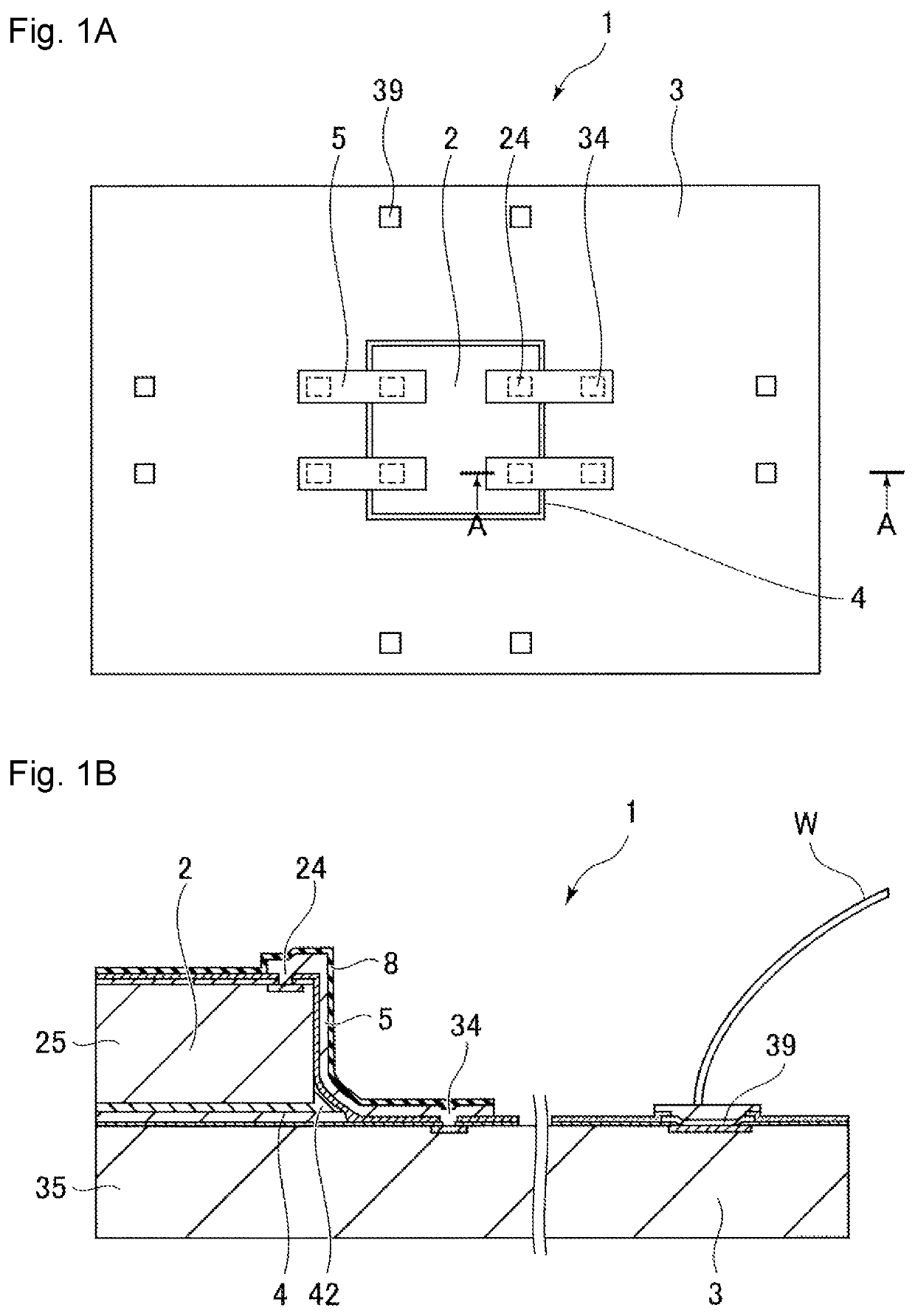
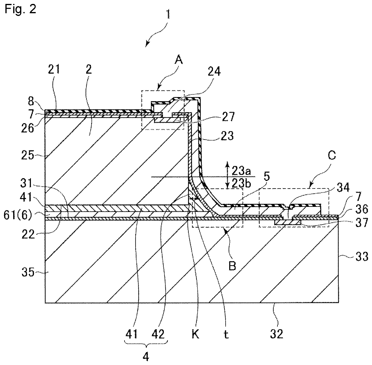
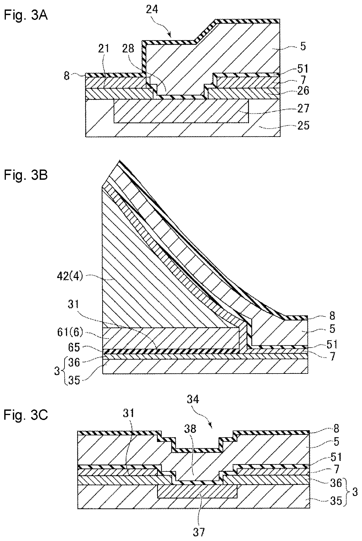
[0024]FIG. 1A is a top view illustrating a stack of electrical components (hereinafter, referred to as stack 1), and FIG. 1B is a cross-sectional view illustrating stack 1 taken along line A-A in FIG. 1A. FIG. 2 is a cross-sectional view illustrating stack 1 in more detail, and FIGS. 3A to 3C are partial cross-sectional views illustrating portion A, portion B, and portion C in FIG. 2 in more detail, respectively.

[0025]First electrical component 2 has an approximately rectangular parallelepiped shape. First electrical component 2 has first surface 21, second surface 22 that is a surface opposite to first surface 21 and first side surfaces 23 that are located between first surface 21 and second surface 22. First electrical component 2 has first electrical connections 24 on first surface 21. First electrical component 2 has first substrate 25 made of silicon, as well as first passivation layer 26 that is provided on first substrate 25. A sensor element, such as a TMR element (not illus...

second embodiment

[0042]Stack 101 according to the second embodiment will be described with reference to FIGS. 8 to 11G. Hereinafter, differences from the first embodiment will be mainly described. The configuration and effects that are not particularly mentioned are the same as those of the first embodiment. FIG. 8 is a top view illustrating stack 101 according to the second embodiment, and FIGS. 9A and 9B are cross-sectional views of stack 101 taken along line A-A and line B-B of FIG. 8, respectively. FIGS. 10A and 10B are partial cross-sectional views illustrating portion D and portion E in FIG. 9A in more detail, respectively. It should be noted that portion A and portion B in FIG. 9A are the same as in the first embodiment. Refer to FIG. 3A to 3C and the above-mentioned description.

[0043]In the present embodiment, second portion 42 of adhesive layer 4 and conductive layer 5 are covered with molding material 9 that is made of an epoxy resin. Conductive pillar 10 is connected to conductive layer 5...


PUM


Abstract

A stack of electrical components has a first electrical component having a first surface, a second surface that is opposite to the first surface and a side surface that is located between the first surface and the second surface; a second electrical component having a third surface on which the first electrical component is mounted, the third surface facing the second surface and forming a corner portion between the third surface and the side surface; an adhesive layer that bonds the first electrical component to the second electrical component, wherein the adhesive layer has a first portion that is located between the second surface and the third surface and a curved second portion that fills the corner portion; and a conductive layer that extends on a side of the side surface, curves along the second portion and extends to the third surface.

Description

BACKGROUND OF THE INVENTIONField of the Invention[0001]The present application is based on, and claims priority from, J.P. Application No. 2018-193174 filed on Oct. 12, 2018, the disclosure of which is hereby incorporated by reference herein in its entirety.[0002]The present invention relates to a stack of electrical components and a method of producing the same, particularly to a stack of electrical components in which an ASIC (application-specific integrated circuit) and a magnetic sensor are stacked.Description of the Related Art[0003]A technique is known in which a package is formed by mounting an electrical component, such as an integrated circuit, a semiconductor element, a MEMS and a magnetic sensor, on another electrical component. U.S. Pat. No. 9,466,580 discloses a semiconductor package in which a semiconductor die (hereinafter, referred to as a first electrical component) is mounted on another semiconductor die (hereinafter, referred to as a second electrical component). ...

Claims


Application Information

Patent Timeline
Patent Type & Authority Patents(United States)
IPC IPC(8): H01L23/00H01L25/18
CPCH01L24/73H01L24/29H01L24/32H01L24/40H01L24/83H01L24/92H01L25/18H01L2224/26145H01L2224/29191H01L2224/32145H01L2224/40106H01L2224/40145H01L2224/73263H01L2224/83855H01L2224/92246H01L21/768H01L25/0657H01L2224/32057H01L2224/32058H01L2224/32148H01L2224/83139H01L2224/83143H01L2224/82101H01L2224/821H01L2224/245H01L2224/24105H01L2224/24146H01L2224/25175H01L2224/24991H01L2224/24998H01L2224/04105H01L2224/73267H01L2224/73203H01L2224/92244H01L2224/0346H01L2224/05147H01L2224/9202H01L2224/94H01L2224/8385H01L24/24H01L24/05H01L24/82H01L2224/2731H01L2224/04026H01L25/50H01L2225/06551H01L2225/06575H01L2225/06555H01L2224/82951H01L2924/01029H01L2924/00014H01L2924/01079H01L2924/01047H01L2924/01013H01L2224/03H01L2224/82H01L2224/83
Inventor HIROTA, YOHEIYAMAZAKI, HIROSHIIWAMA, HITOSHITAKAHASHI, YUSUKE
Owner TDK CORPARATION
Why Eureka
Try Eureka