Array substrate and display device

a display device and substrate technology, applied in the field of display, can solve the problems of reducing wasting material and space, and the interlayer dielectric layer overhanging the curved wire to easily break, so as to improve the service life of the product, maintain uniform resistance of each fan-out wire, and improve the service life

Active Publication Date: 2021-10-05
WUHAN CHINA STAR OPTOELECTRONICS SEMICON DISPLAY TECH CO LTD
View PDF11 Cites 1 Cited by
  • Summary
  • Abstract
  • Description
  • Claims
  • Application Information

AI Technical Summary

Benefits of technology

[0017]In the present invention, an array substrate and a display device are provided. The resistance of each fan-out wire is kept uniform by connecting polysilicon resistors in series, and the magnitude of the resistance can be adjusted by changing the length and size of the polysilicon. In this way, the resistance is kept substantially consistent and it does not cause breakage of the interlayer dielectric layer, therefore, it also does not cause a short circuit between the fan-out wire and the source and drain electrodes on the interlayer dielectric layer, thereby improving the service life of the product. The way of eliminating the windings renders the structure simpler, saves raw materials and reduces costs.

Problems solved by technology

This method not only wastes material and space but also easily causes the interlayer dielectric layer overlaying the curved wire to easily rupture because a curvature of the edge of the inner side of the curved wire is relatively large.
As a result, a short circuit occurs between the fan-out wire and the source and drain electrodes on the interlayer dielectric layer, which greatly reduces the service life of the product.

Method used


Image

  • Array substrate and display device
  • Array substrate and display device

Examples


Embodiment Construction

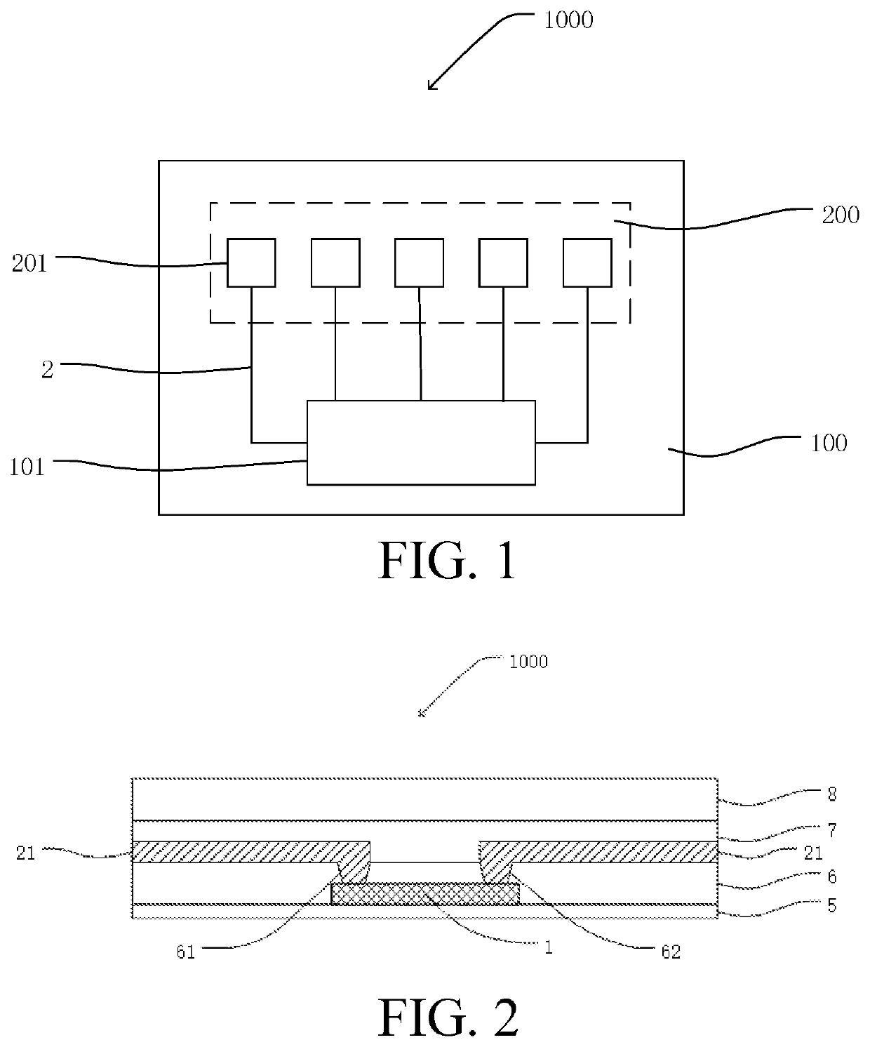
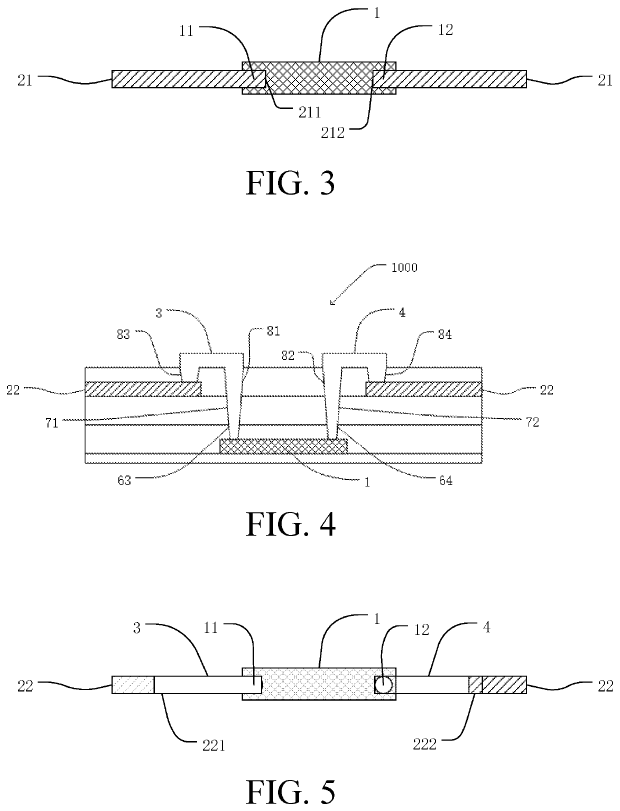
[0025]The technical solutions in the embodiments of the present invention will be clearly and completely described as follows with reference to the drawings in the embodiments of the present invention. Obviously, the described embodiments are a part of the embodiments in the invention, not all of them. Based on the embodiments of the present invention, all other embodiments obtained by those skilled in the field without doing any creative activity are within the claimed scope of the present invention.

[0026]In the drawings, components having the same structure are denoted by the same reference numerals. Components that are structurally or functionally similar are denoted by like reference numerals. The dimensions and thickness of each component shown in the drawings are arbitrarily shown, and the invention does not limit the size and thickness of each component. In order to make the illustration clearer, some parts of the drawings appropriately exaggerate the thickness of the compone...


PUM

PropertyMeasurementUnit
areaaaaaaaaaaa
insulating dielectricaaaaaaaaaa
flexibilityaaaaaaaaaa

Abstract

An array substrate and a display device are provided. The array substrate is provided with a display area and a non-display area, and the array substrate further includes a plurality of thin film transistors, a driving circuit, a plurality of polysilicon resistors, and a plurality of fan-out wires. The thin film transistor array is arranged in the display area, and each thin film transistor is provided with an input end. The driving circuit corresponds to the non-display area, and the driving circuit is provided with an output end. The polysilicon resistors and the fanout wires correspond to the non-display area. Two ends of each polysilicon resistor are respectively connected to the input end of a corresponding thin film transistor and the output end of the driving circuit through a corresponding fanout wire.

Description

FIELD OF INVENTION[0001]The present invention relates to the field of display, and in particular to an array substrate and a display device.BACKGROUND OF INVENTION[0002]With the rapid development of technology, people are increasingly relying on information exchange and delivery. As the main carrier and foundation for information exchange and delivery, display devices have become the hotspots and highlands that many scientists in the fields of information and optoelectronics are competing for.[0003]The advent of AMOLED (active matrix organic light emitting diode) is a big breakthrough in the field of display technology. Due to its self-illumination principle, there is no need for backlights, color filters, and other components. AMOLED is lighter and thinner than LCD (liquid crystal display), consumes less energy and is less susceptible to damage than a glass substrate because of its flexibility.[0004]In AMOLED, the driving circuit transmits signals to the display area through the fa...

Claims


Application Information

Patent Timeline
Patent Type & Authority Patents(United States)
IPC IPC(8): H01L27/00H01L27/12
CPCH01L27/124H01L27/1248H10K59/00H10K59/12H10K59/131H01L27/1255
Inventor MA, WEIXIN
Owner WUHAN CHINA STAR OPTOELECTRONICS SEMICON DISPLAY TECH CO LTD
Why Eureka
Try Eureka