Supercharge Your Innovation With Domain-Expert AI Agents!

Display panel and chip suitable for the display panel

a display panel and chip technology, applied in the field of display technologies, can solve the problems of large influence of impedance on impedance-sensitive signals, and achieve the effect of reducing the influence of the impedance of the signal transmission lin

Active Publication Date: 2022-02-15
WUHAN CHINA STAR OPTOELECTRONICS TECH CO LTD
View PDF1 Cites 0 Cited by
  • Summary
  • Abstract
  • Description
  • Claims
  • Application Information

AI Technical Summary

Benefits of technology

This design effectively reduces the influence of signal transmission line impedance on signal quality by optimizing the distance, impedance, and arrangement of transmission lines, ensuring better signal integrity across the display panel.

Problems solved by technology

Thus, the impedance-sensitive signal is greatly affected by the impedance of the traces.

Method used


Image

  • Display panel and chip suitable for the display panel
  • Display panel and chip suitable for the display panel

Examples


Embodiment Construction

[0033]The term “embodiment” as used in this specification means an example, a sample or an illustration. In addition, the articles “a” or “an” generally can be interpreted as “one or more,” unless otherwise specified or the singular form can be clearly determined.

[0034]The display panel of the present invention may be a thin film transistor liquid crystal display (TFT-LCD), an organic light emitting diode (OLED), or the like.

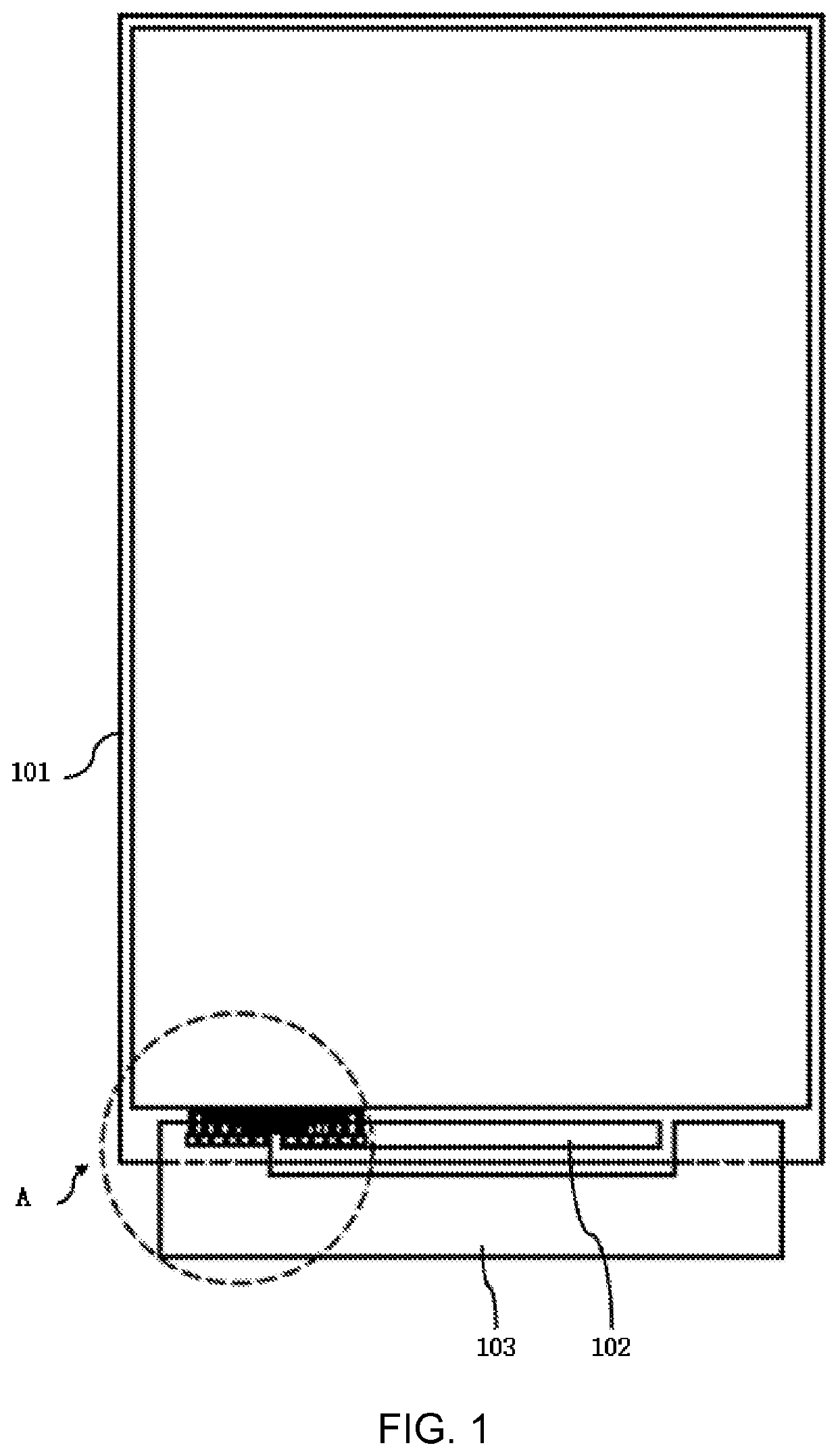
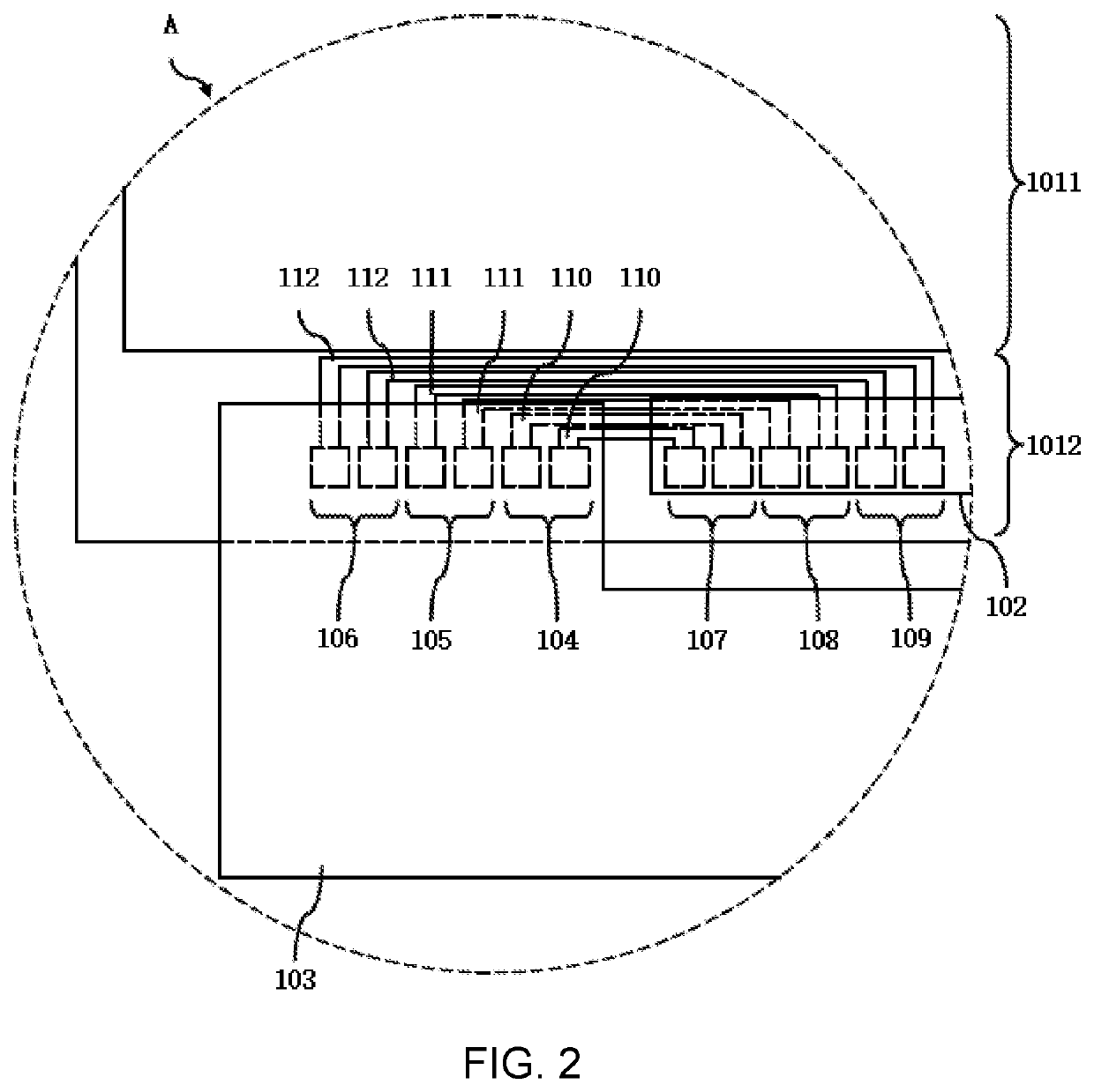
[0035]Please refer to FIG. 1 and FIG. 2. FIG. 1 is a schematic view of a display panel of the present invention, and FIG. 2 is a schematic view of an area A in the display panel shown in FIG. 1.

[0036]The display panel comprises a panel body 101, a potential signal transmission circuit for transmitting a potential signal, a first frequency signal transmission circuit for transmitting a first frequency signal, and a second frequency signal transmission circuit for transmitting a second frequency signal. The panel body 101 can be, for example, a chip on glass (COG)...


PUM

PropertyMeasurementUnit
frequencyaaaaaaaaaa
frequencyaaaaaaaaaa
angleaaaaaaaaaa

Abstract

The present invention provides a display panel and a chip. A frequency of a signal in a first frequency signal transmission line is greater than a frequency of a signal in a second frequency signal transmission line. A distance between a first signal input pad and a first signal output pad is smaller than a distance between a second signal input pad and a second signal output pad, and the distance between the second signal input pad and the second signal output pad is smaller than a distance between a third signal input pad and a third signal output pad. The invention can reduce the influence of the impedance of the signal transmission line on the signal.

Description

CROSS-REFERENCE TO RELATED APPLICATIONS[0001]This application is a 371 U.S. National Stage of International Application No. PCT / CN2019 / 086309, filed on May 10, 2019, which claims priority to Chinese Application No. 201910299079.5, filed on Apr. 15, 2019. The entire disclosures of the above applications are incorporated herein by reference.FIELD OF INVENTION[0002]The present invention relates to the field of display technologies, and in particular, to a display panel and a chip suitable for the display panel.BACKGROUND OF INVENTION[0003]Conventional chip on glass (COG) modules are generally provided with conductive pads for electrically connecting to pins of the chip, and the conductive pads are electrically connected to the traces.[0004]In practice, the inventors have found that prior arts have at least the following problems:[0005]As the number of conductive pads (pins of chips) increase, the conductive pads at the ends away from the chip need to be connected with longer traces. Th...

Claims


Application Information

Patent Timeline
Patent Type & Authority Patents(United States)
IPC IPC(8): H01L27/12G02F1/1345H01L25/18H01L27/32
CPCH01L27/124G02F1/13452G02F1/13456H01L25/18H01L27/3276G02F1/136286G02F1/133G09F9/33H10K59/131
Inventor ZOU, GONGHUA
Owner WUHAN CHINA STAR OPTOELECTRONICS TECH CO LTD
Features
  • R&D
  • Intellectual Property
  • Life Sciences
  • Materials
  • Tech Scout
  • Unparalleled Data Quality
  • Higher Quality Content
  • 60% Fewer Hallucinations
Learn More