Separable modules PCB modules

a technology of pcb modules and separable modules, which is applied in the direction of printed circuits, circuit bendability/stretchability, programmable/customizable/modifiable circuits, etc. it can solve the problems of prior art systems that do not provide the desired solutions for practical applications, and essentially do not provide scalable systems. , to achieve the effect of reducing the chance, improving stock management, and reducing the chance of shortening

Active Publication Date: 2022-03-15
SIGNIFY HLDG BV
View PDF13 Cites 0 Cited by
  • Summary
  • Abstract
  • Description
  • Claims
  • Application Information

AI Technical Summary

Benefits of technology

[0006]Such PCB allows an improved stock management, as a large PCB may be stored, and, when desired, one or more PCB areas may be snapped away to provide a PCB (module)(smaller than the PCB from which it was snapped away), e.g. for use in a (lighting) system. Further, such PCB allows snapping away PCB elements that are at least to some extend protected from short circuiting due to undesired contact with electrically conductive elements in a system wherein the PCB element is applied. This protection may be provided by the fact that the electrically conductive track ends at a recessed part and adjacent therefrom a projecting part is available. The latter part may facilitate reduction of the chance that the conductive track, which is now accessible at the edge of the snapped away PCB comprising part or of the remaining PCB of which the PCB area comprising part was snapped away), comes into undesired contact with another electrically conductive element, such as an earth. Further, in embodiments such PCB allows scalability, as the larger unit may be used as such, but may also be divided in two (or more) snapped away PCB modules, that may also be functionally used. Hence, the present invention provides separable PCB modules.
[0007]As known in the art, a printed circuit board may mechanically support and electrically connect electronic components or electrical components using conductive tracks, pads and other features etched from one or more sheet layers of copper laminated onto and / or between sheet layers of a non-conductive substrate (shortly indicated as “track” or “conductive track”). Components are generally soldered onto the PCB to both electrically connect and mechanically fasten them to it. For instance, a basic PCB may consist of a flat sheet of insulating material and a layer of copper foil, laminated to the substrate. Chemical etching divides the copper into separate conducting lines called tracks or circuit traces, pads for connections, vias to pass connections between layers of copper, and features such as solid conductive areas for EM shielding or other purposes. The tracks function as wires fixed in place, and are insulated from each other by air and the board substrate material. The surface of a PCB may have a coating that protects the copper from corrosion and reduces the chances of solder shorts between traces or undesired electrical contact with stray bare wires. For its function in helping to prevent solder shorts, the coating is called solder resist.
[0026]The use of a perforation line has as advantage that the electrically conductive track(s) is not interrupted in such a way that electrical conductivity is blocked. The electrical conductivity is maintained between both sides of the perforation line, allowing the functional use of both the PCB areas at both sides of the perforation line. Nevertheless, such perforation line also allows a relatively controlled snapping away of a first PCB area from an adjacent second PCB area. Hence, the perforation line does not (fully) interrupt the electrically conductive track, but intercepts the electrically conductive track (without essentially affecting its functionality). As the perforation line may include a plurality of holes, the holes interrupt the conductive track, but the areas between two holes provide effectively an uninterrupted electrically conductive track.
[0028]By snapping away a PCB area or PCB area comprising part, part of the electrically conductive track becomes accessible at edge of the PCB area. This may impose risks, such as short circuit, etc. Hence, the present invention may provide a protection against such risks.

Problems solved by technology

The above cited prior art does essentially not provide a scalable system, but provides identical independent PCBs that are interconnected.
Hence, prior art systems do not provide the desired solutions for practical applications.

Method used


Image

  • Separable modules PCB modules
  • Separable modules PCB modules
  • Separable modules PCB modules

Examples


Embodiment Construction

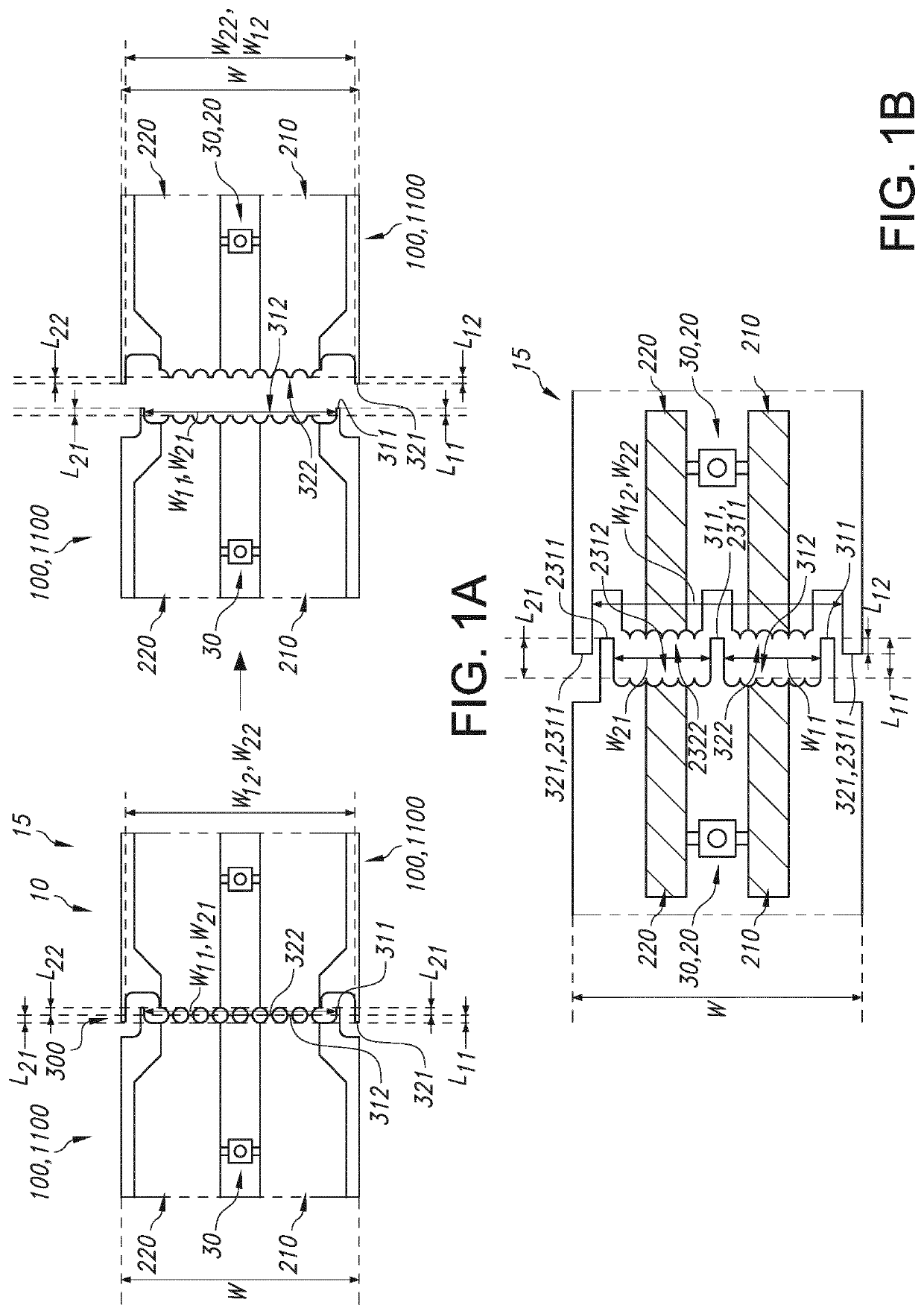
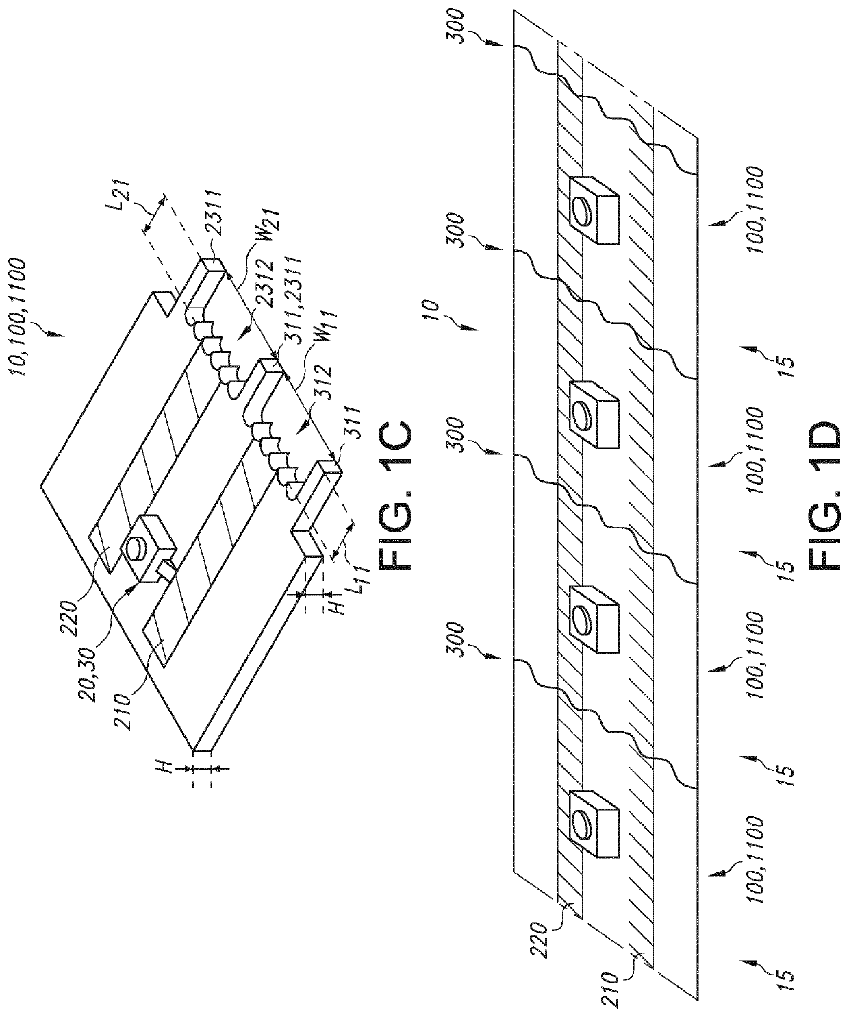
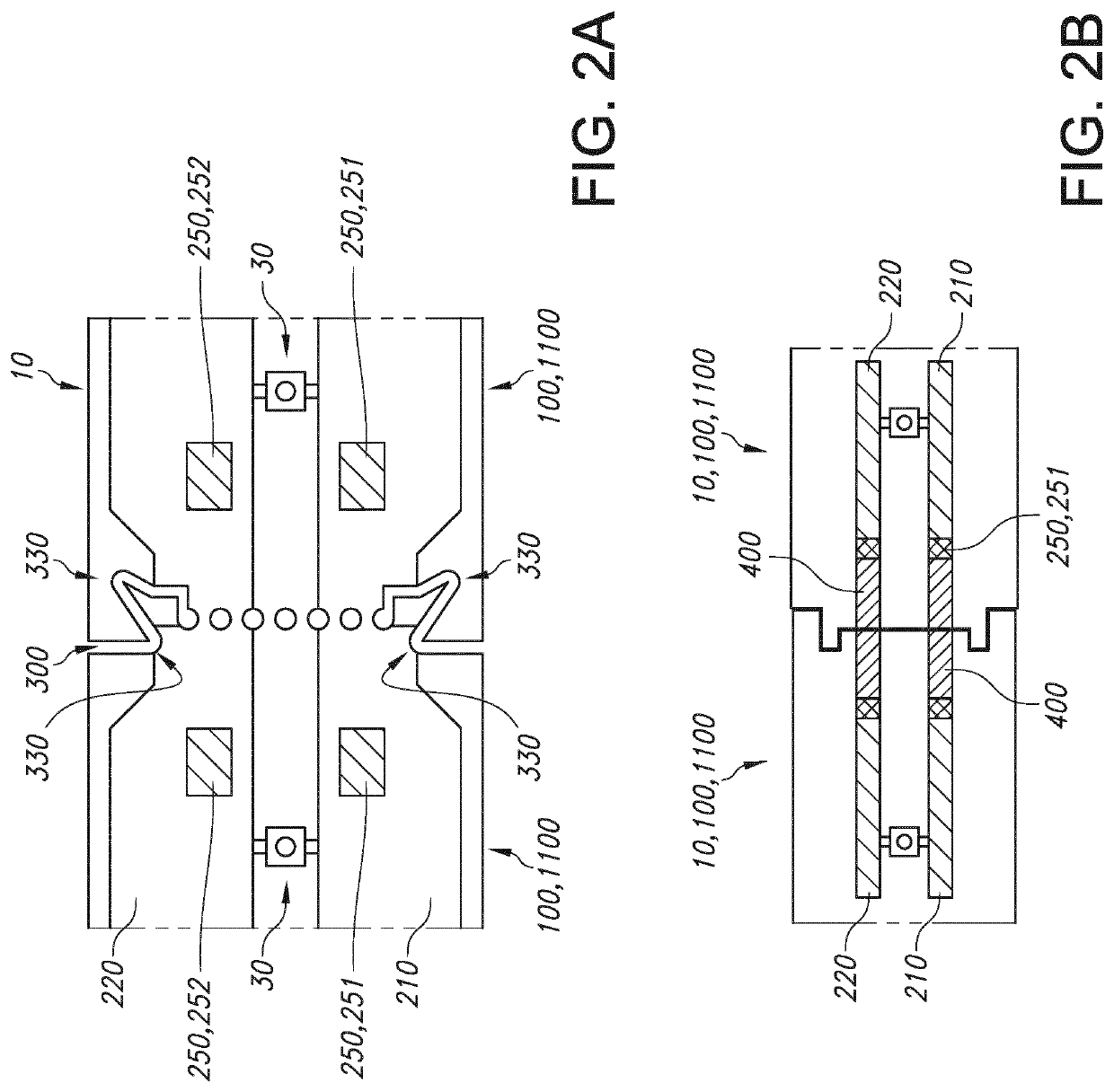
[0064]FIG. 1a very schematically depicts an embodiment of a printed circuit board 10 as described herein.

[0065]The printed circuit board 10 in this embodiment includes a first electrically conductive track 210. The printed circuit board 10 comprises a set 15 of two printed circuit board areas 100 both comprising a part of the first electrically conductive track 210. The printed circuit board 10 further comprises a perforation line 300 between the two printed circuit board areas 100. This can be used for customizing the printed circuit board 10 into two physically separated printed circuit board area comprising parts 1100, as shown on the right of the drawing.

[0066]The perforation line 300 is configured as a non-straight line. The perforation line 300 comprises relative to one of the printed circuit board areas 100, and in a plane of the printed circuit board 10, a first projecting part 311 and a first recessed part 312. The first recessed part 312 is recessed relative to the first p...


PUM


Abstract

The invention provides a printed circuit board (10) including a first electrically conductive track (210), wherein the printed circuit board (10) comprises a set (15) of two printed circuit board areas (100) both comprising a part of the first electrically conductive track (210), wherein printed circuit board (10) further comprises a perforation line (300) between the two printed circuit board areas (100) for customizing the printed circuit board (10) into two physically separated printed circuit board area comprising parts (1100), wherein the perforation line (300) is configured as a non-straight line, wherein the perforation line (300) comprises relative to one of the printed circuit board areas (100), and in a plane of the printed circuit board (10), a first projecting part (311) and a first recessed part (312), wherein the first recessed part (312) is recessed relative to the first projecting part (311), wherein the first electrically conductive track (210) is intercepted by the perforation line (300) at the first recessed part (312).

Description

CROSS-REFERENCE TO PRIOR APPLICATIONS[0001]This application is the U.S. National Phase application under 35 U.S.C. § 371 of International Application No. PCT / EP2019 / 077025, filed on Oct. 7, 2019, which claims the benefit of European Patent Application No. 18199964.0, filed on Oct. 11, 2018. These applications are hereby incorporated by reference herein.FIELD OF THE INVENTION[0002]The invention relates to a printed circuit board (PCB), to a kit of parts comprising such printed circuit board, and to a method of functionally coupling printed circuit board area comprising parts.BACKGROUND OF THE INVENTION[0003]The use of perforated printed circuit boards (PCBs) is known in the art. U.S. Pat. No. 3,780,431, for instance, describes a pallet which is made up of a number of printed circuit boards, the boards being perforated at their interconnected edges whereby each printed circuit board can be easily snapped apart at a selected stage of assembly. In an embodiment, the printed circuit boar...

Claims


Application Information

Patent Timeline
Patent Type & Authority Patents(United States)
IPC IPC(8): H05K1/02H05K3/36
CPCH05K1/0278H05K1/0293H05K3/368H05K2201/0909H05K2201/09036H05K2201/09063H05K2201/09127H05K2201/10106H05K2203/302H05K3/0052H05K3/0097H05K3/3442H05K2201/0394H05K2201/09145H05K2201/09172H05K2201/09181H05K2201/209
Inventor LEERMAKERS, REMCO CHRISTIANUS WILHELMUSVAN KEMPEN, FRANK WALTERUS MARIE
Owner SIGNIFY HLDG BV
Why Eureka
Try Eureka