

Semiconductor device
- Summary
- Abstract
- Description
- Claims
- Application Information
AI Technical Summary
Benefits of technology
Problems solved by technology
Method used
Image

Examples
Embodiment Construction
[0018]Exemplary embodiments of the present inventive concepts will now be described more fully with reference to the accompanying drawings, in which exemplary embodiments are show n.
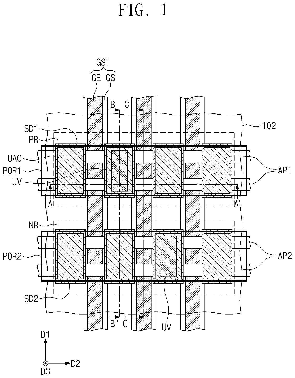
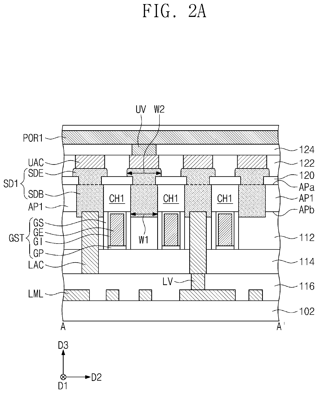
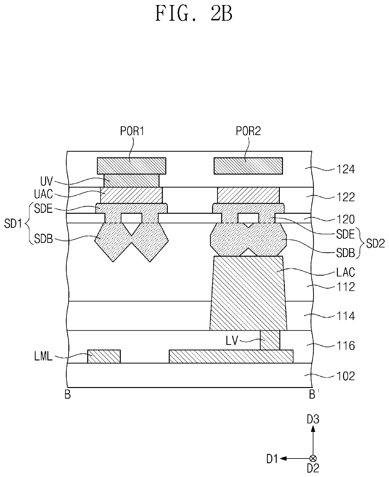
[0019]18) FIG. 1 is a top plan view illustrating a semiconductor device according to an exemplary embodiment of the present inventive concepts. FIGS. 2A to 2C are cross-sectional views taken along lines A-A′, B-B′, and C-C′, respectively, of FIG. 1 according to exemplary embodiments of the present inventive concepts.
[0020]Referring to FIGS. 1 and 2A to 2C, a lower substrate 102 may include a p-channel metal-oxide field-effect transistor (“PMOSFET”) region PR and an n-channel metal-oxide field-effect transistor (“NMOSFET”) region NR. The lower substrate 102 may be a semiconductor substrate, which is formed of or includes silicon, germanium, or silicon-germanium, or a compound semiconductor or substrate. For example, the lower substrate 102 may be a silicon wafer. However, exemplary embodiments of the pres...
PUM
 Abstract
Description
Claims
Application Information