Nonvolatile memory device and method of fabricating the same

Active Publication Date: 2018-03-01
KWON EUIPIL
View PDF12 Cites 2 Cited by
  • Summary
  • Abstract
  • Description
  • Claims
  • Application Information

AI Technical Summary

Benefits of technology

[0016]Embodiments of the inventive concept provide a memory cell capable of storing data smaller area to obtain a higher integration density than in the co

Problems solved by technology

According to the conventional techniques, since a MOS transistor and a storage element should be formed in a memory cell, a fabrication process becomes re

Method used


Image

  • Nonvolatile memory device and method of fabricating the same
  • Nonvolatile memory device and method of fabricating the same
  • Nonvolatile memory device and method of fabricating the same

Examples


Example

[0073]The inventive concept will now be described more fully hereinafter with reference to the accompanying drawings, in which embodiments of the inventive concept are shown. This inventive concept may, however, be embodied in different forms and should not be construed as limited to the embodiments set forth herein. Rather, these embodiments are provided so that this disclosure is thorough and complete and fully conveys the scope of the inventive concept to one skilled in the art.

[0074]The following detailed description is merely exemplary in nature and is not intended to limit the application and uses contemplated herein. Furthermore, there is no intention to be bound by any theory presented in the preceding background or the following detailed description.

[0075]The inventive concept will now be described more fully hereinafter with reference to the accompanying drawings, in which embodiments of the inventive concept are shown.

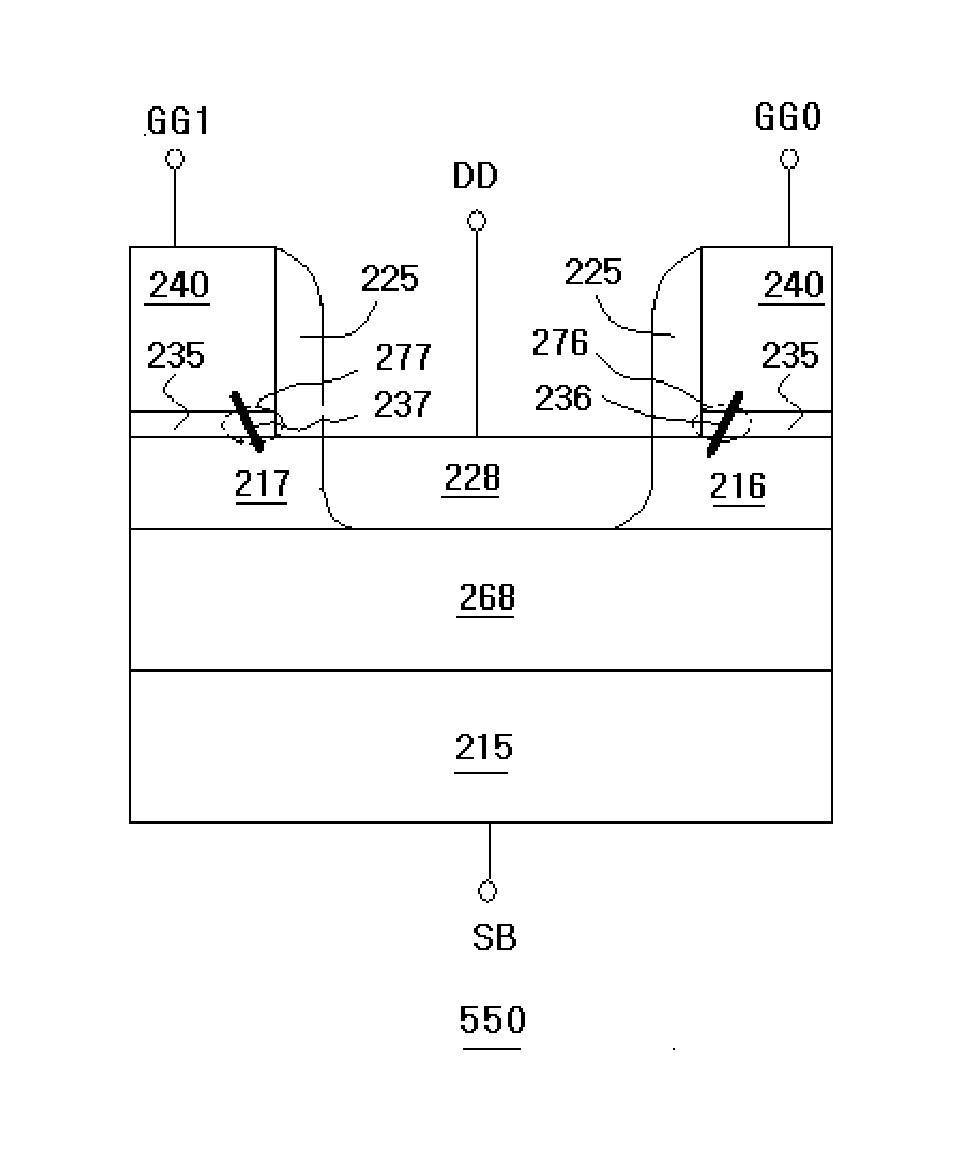
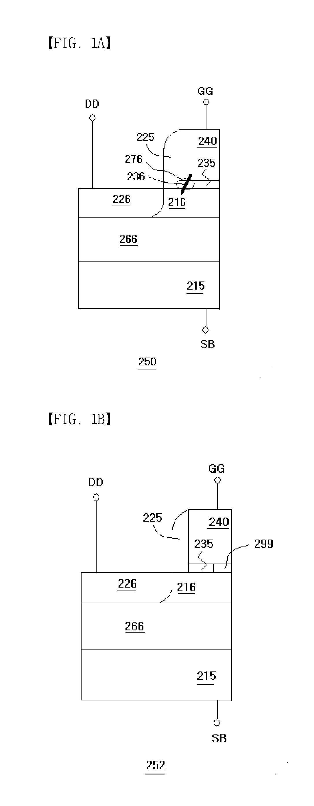
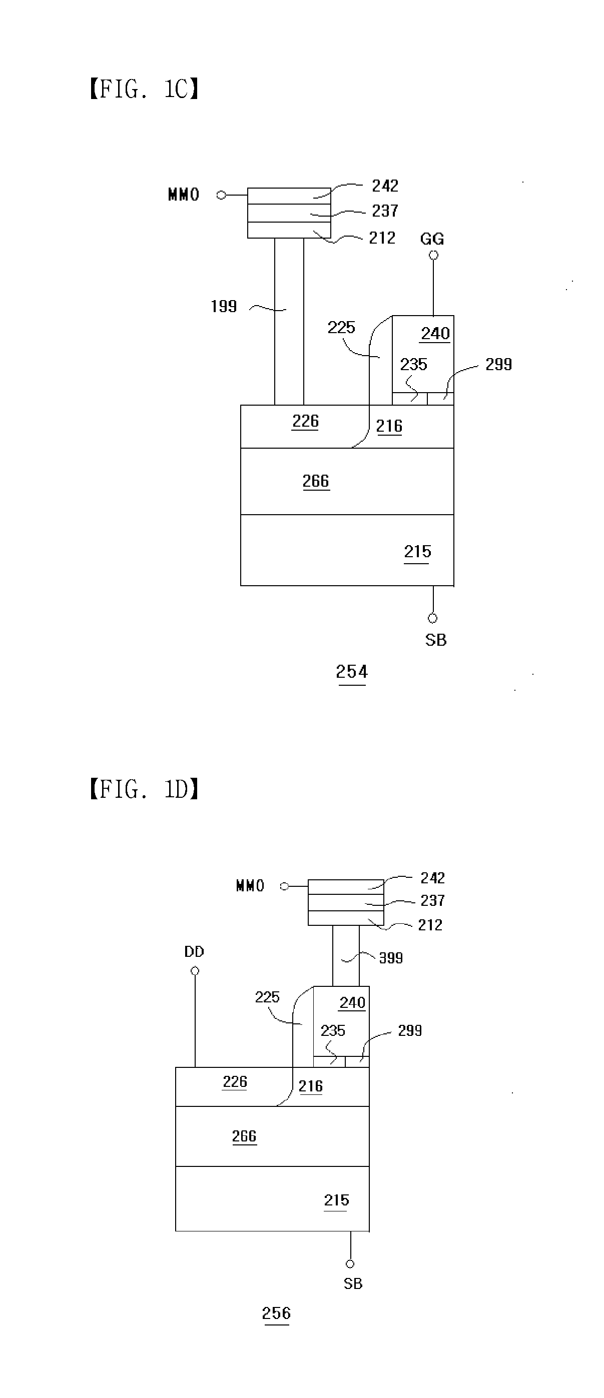
[0076]A structure according to the inventive concept m...


PUM


Abstract

The nonvolatile memory device includes a semiconductor substrate, a first and a second diffusion regions formed under a surface of the semiconductor substrate, a storage layer formed on the semiconductor substrate, a gate stacked on the storage layer, wherein the first diffusion region may at least one of active regions being separated by a part of the semiconductor substrate forming a channel region., wherein the second diffusion region may include an active region intersecting the gate insulating layer, wherein the storage layer may include an insulating layer or a variable resistor, and may service as a data storage layer to store data, and may be selected by a structure including the first and the second diffusion regions.

Description

BACKGROUND1. Field[0001]Embodiments of the inventive concept relate to a nonvolatile memory device and a method of fabricating the same and, more particularly, to a nonvolatile memory device including a part of a transistor serving as a basic structure, an insulating layer or a variable resistor.2. Description of Related Art[0002]A conventional art disclosed in US Patent Publication No. 20130249017 related a nonvolatile memory device and a method of fabricating the same. The nonvolatile memory device includes a memory cell having a transistor in which an insulating isolation layer is formed in a channel region. The nonvolatile memory device includes a metal-oxide-semiconductor (MOS) transistor as a basic component. An insulating isolation layer is formed in at least a channel region, and a gate insulating layer includes an insulating layer or a variable resistor and serves as a data storage. A gate includes a metal layer formed in a lower portion thereof. A first source and a drain ...

Claims


Application Information

Patent Timeline
IPC IPC(8): H01L27/24H01L29/872H01L27/06H01L27/22
CPCH01L27/2409H01L29/872H01L27/226H01L27/2445H01L27/224H01L27/0629H10B63/20H10N70/253H10N70/821H10N70/828H10N70/231H10B61/10H10B61/20H10B63/24H10B63/32H10N70/801H10N70/823H10N70/826
Inventor KWON, EUIPIL
Owner KWON EUIPIL
Why Eureka
Try Eureka