Groove capacitor and its manufacture

A technology of capacitors and trenches, applied in semiconductor/solid-state device manufacturing, circuits, electrical components, etc., can solve problems such as damaging dielectric chemical reactions, achieve low wire resistance, fast access time, and increase performance.

Inactive Publication Date: 2005-02-23
INFINEON TECH AG
View PDF0 Cites 3 Cited by
  • Summary
  • Abstract
  • Description
  • Claims
  • Application Information

AI Technical Summary

Problems solved by technology

At this point in time, the internal electrodes consist of systems having a resistance in the range below 1000 x 10 -6 ohms/cm of doped polysilicon, and since the resistance depends on the cross-sectional area of ​​a conductor, one of the trench capacitor structures is further miniaturized, and thus the miniaturization of the internal electrodes leads to the internal A very high non-reactive resistance of the electrodes and, resulting in the electrically active section of the inner electrode being lower than the neck regi

Method used


Image

  • Groove capacitor and its manufacture
  • Groove capacitor and its manufacture
  • Groove capacitor and its manufacture

Examples


Embodiment Construction

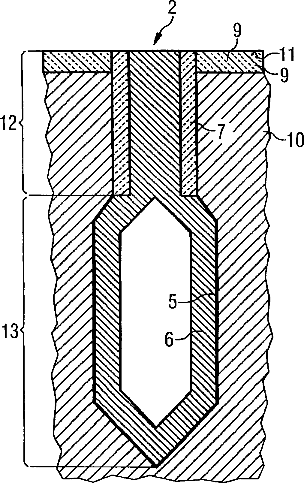
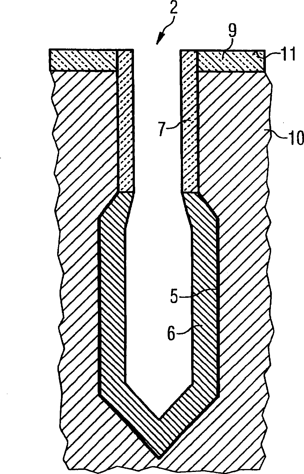
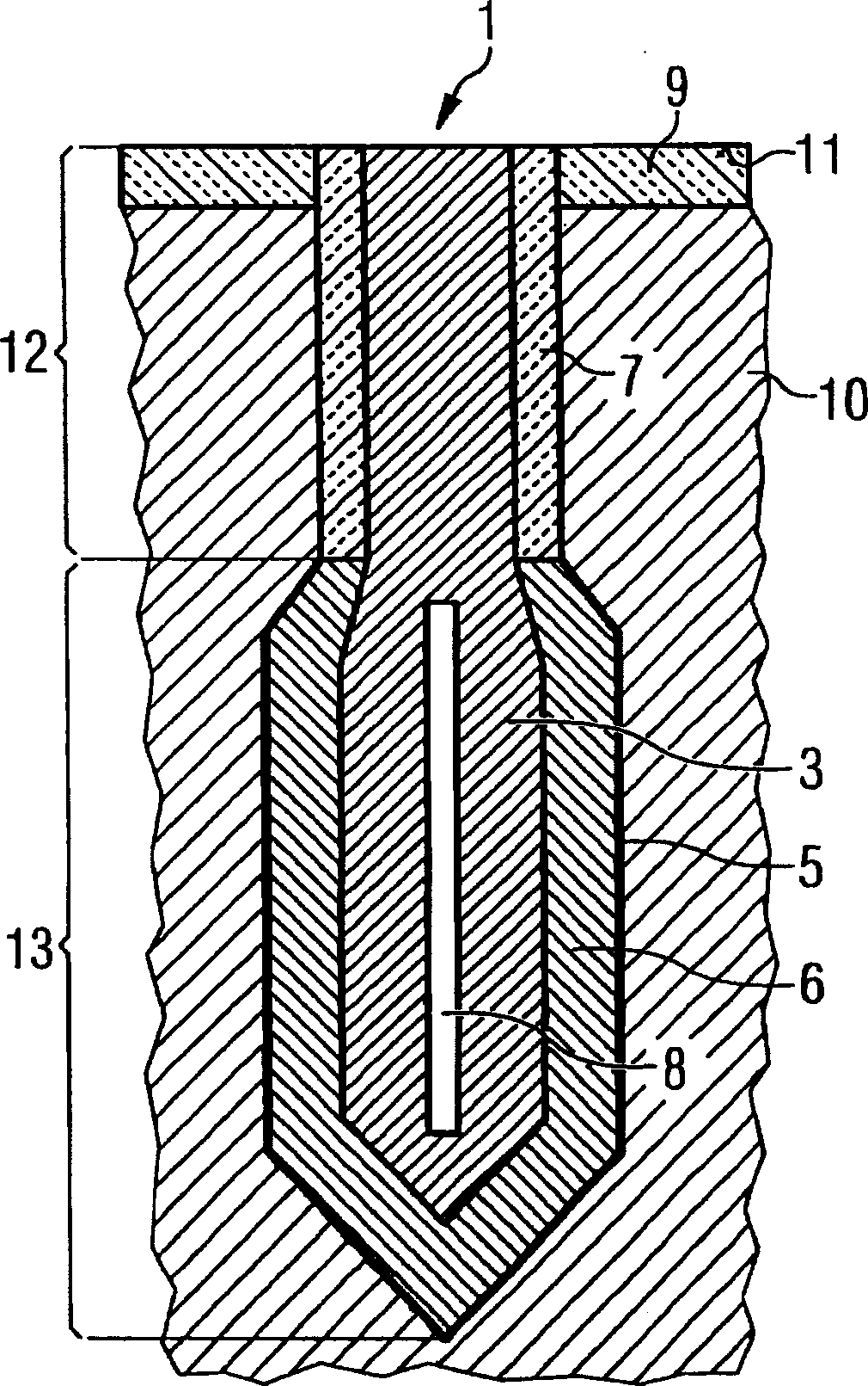
[0031] In order to manufacture a trench capacitor 1 in a semiconductor substrate 10, a hole trench 2 is introduced into the semiconductor substrate 10 from a substrate surface 11, and an external electrode, for example, as a "buried plate" , is, for example, provided in a section of the semiconductor substrate 10 adjacent to the hole trench 2 by depositing a region in the semiconductor substrate 10, furthermore, the hole trench 2 There is an active region 13 extending into the semiconductor substrate 10 and lined with a dielectric layer 5 such as, for example, metal oxides and oxides of rare earths, such as Al 2 o 3 , HfO 2 , ZrO 2 , La 2 o 3 , can be provided as the dielectric layer 5 . Next, a neck region 12 is located between the substrate surface 11 and the active region 13 . In this exemplary embodiment of the method according to the invention, however, a silicon nitride layer 9 is provided on the semiconductor substrate 10, which in this case comprises crystalline ...


PUM

PropertyMeasurementUnit
Thicknessaaaaaaaaaa

Abstract

A method for fabricating a trench capacitor in a semiconductor substrate with a low-impedance inner electrode for use in memory cells of memory devices. A separating layer is provided on a dielectric layer in the active region of the trench capacitor. Afterward, a low-impedance inner electrode made of metal or a metal compound is introduced both in the active region and in the collar region lined with an insulation layer.

Description

technical field [0001] The present invention relates to a method for manufacturing a trench capacitor in a semiconductor substrate, wherein a hole trench is introduced into the semiconductor substrate from a substrate surface, and a External electrodes are provided in a section of the semiconductor substrate adjacent to the hole trench, furthermore, the hole trench is lined with a dielectric layer in an active region extending into the semiconductor substrate, and A collar region between the substrate surface and the active region is lined with an insulating layer. Additionally, the present invention is additionally related to a trench capacitor. Background technique [0002] When manufacturing semiconductor circuit devices such as DRAM (Dynamic Random Access Memory, dynamic random access memory) memory devices, one of the main considerations is, for example, to increase the bulk density. Usually, in this case, it is an attempt to To increase the number of switching elemen...

Claims


Application Information

Patent Timeline
IPC IPC(8): H01L21/02H01L21/334H01L21/8242H01L27/108H01L29/94
CPCH01L29/945H01L29/66181
Inventor H·塞德A·塞格S·库德卡M·古茨彻
Owner INFINEON TECH AG
Why Eureka
Try Eureka