Wiring board and method for manufacturing wiring board

a manufacturing method and wiring board technology, applied in the field of wiring boards, can solve the problems of easy damage and readily occurring defects such as wiring board damage, and achieve the effect of suppressing defects in the wiring board

Active Publication Date: 2022-03-22
DAI NIPPON PRINTING CO LTD +1
View PDF21 Cites 0 Cited by
  • Summary
  • Abstract
  • Description
  • Claims
  • Application Information

AI Technical Summary

Benefits of technology

[0004]The wiring board includes not only a section that is resistant to deformation such as extension or contraction but also a section that is easily damaged due to deformation. Hence, when a circuit is provided on substrate in a pre-extended state, defects such as damage to the wiring board readily occurs.
[0005]The purpose of the embodiment of the present disclosure is to provide a wiring board and a method for manufacturing the wiring board that enable the foregoing problems to be resolved effectively.
[0028]According to the embodiment of the present disclosure, it is possible to suppress defects in the wiring board caused by extension and contraction of the substrate.

Problems solved by technology

The wiring board includes not only a section that is resistant to deformation such as extension or contraction but also a section that is easily damaged due to deformation.
Hence, when a circuit is provided on substrate in a pre-extended state, defects such as damage to the wiring board readily occurs.

Method used


Image

  • Wiring board and method for manufacturing wiring board
  • Wiring board and method for manufacturing wiring board
  • Wiring board and method for manufacturing wiring board

Examples


first modification example

[0142]Although the example in which the reinforcing member 30 is positioned on the second surface 22 side of the substrate 20 is illustrated in the foregoing embodiment, the present disclosure is not limited to or by this example. The reinforcing member 30 may be provided on the first surface 21 side of the substrate 20. For example, as illustrated in FIG. 8, the first reinforcing part 31 of the reinforcing member 30 may be positioned between the first surface 21 of the substrate 20 and the electronic component 51. In the example illustrated in FIG. 8, the first reinforcing part 31 is positioned on the second surface 42 of the support substrate 40. Although not illustrated, the second reinforcing part 32 of the reinforcing member 30 may also be provided on the second surface 42 of the support substrate 40.

[0143]FIG. 9 is a cross-sectional view illustrating an enlargement of an example of the wiring 52 of the wiring board 10 illustrated in FIG. 8, and peripheral constituent elements ...

second modification example

[0149]Although the example in which the reinforcing member 30 is positioned on either the second surface 22 of the substrate 20 or the second surface 42 of the support substrate 40 is illustrated in the foregoing embodiment and first modification example, the present disclosure is not limited to or by this example. As illustrated in FIG. 11, the first reinforcing part 31 of the reinforcing member 30 may be positioned either on the second surface 22 side of the substrate 20, or between the first surface 21 of the substrate 20 and the electronic component 51. In the example illustrated in FIG. 11, the wiring board 10 includes a first reinforcing part 31 positioned on the second surface 22 of the substrate 20 and a first reinforcing part 31 positioned on the second surface 42 of the support substrate 40. Although not illustrated, the second reinforcing part 32 of the reinforcing member 30 may also be provided on the second surface 22 of the substrate 20 and on the second surface 42 of ...

third modification example

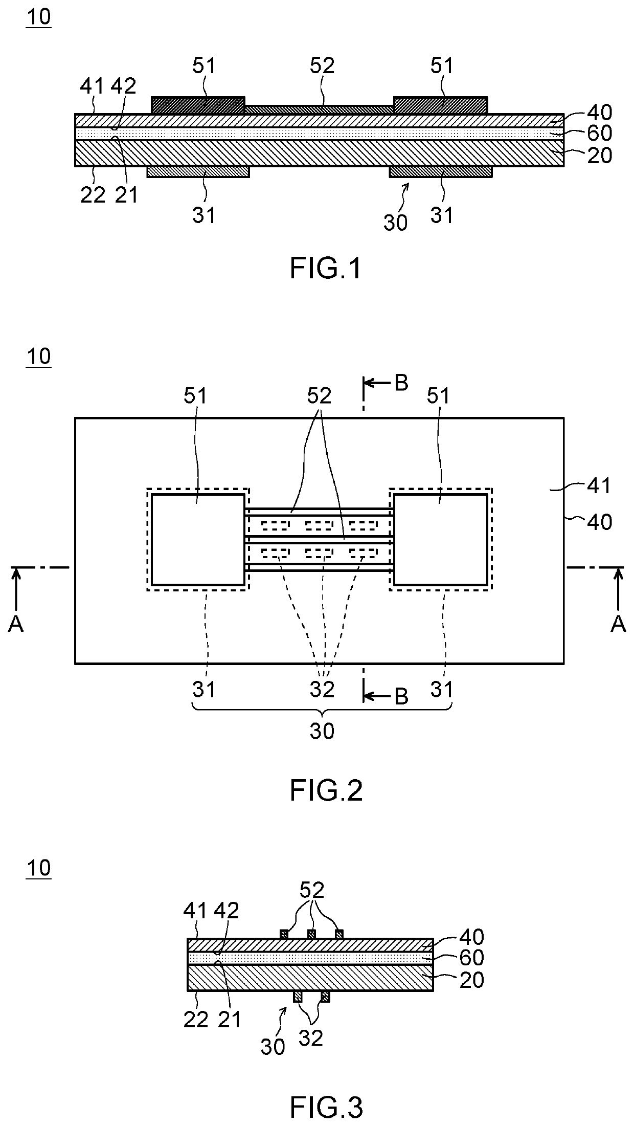
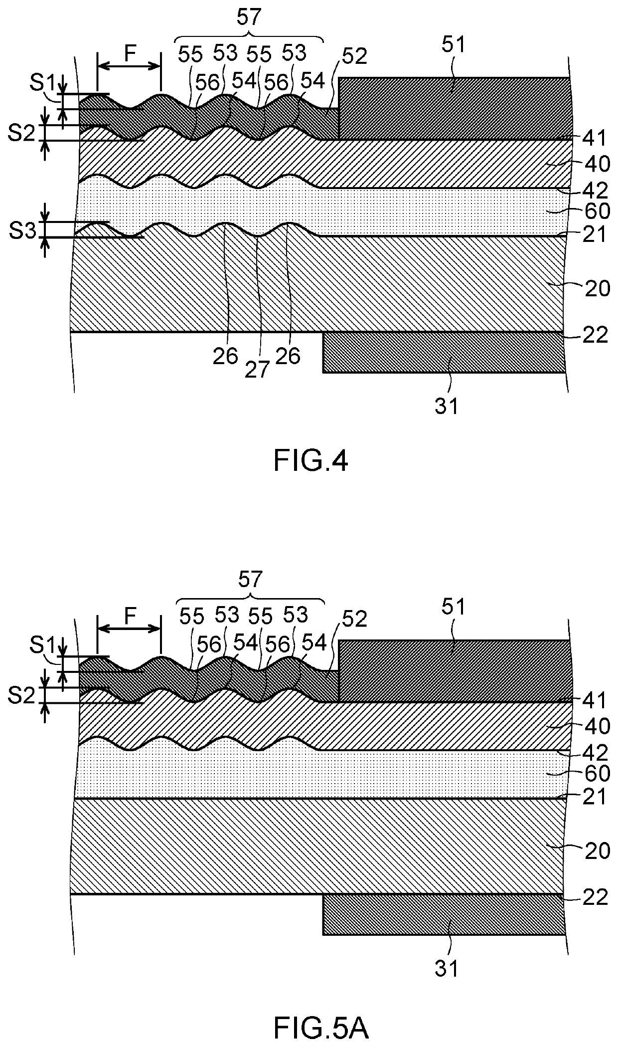
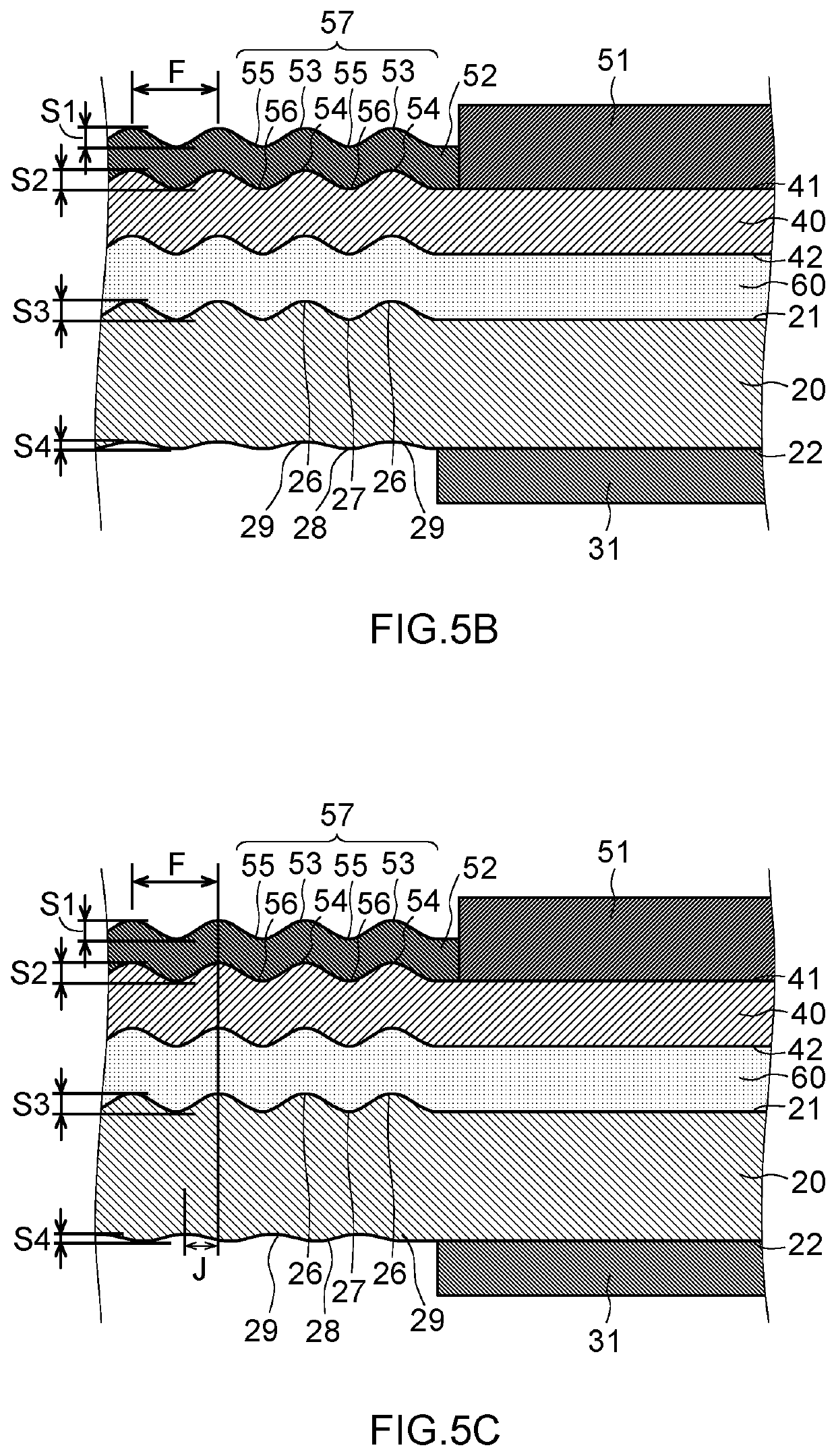
[0156]In the foregoing embodiment and modification examples, the example in which the electronic component 51 and wiring 52 are supported by the support substrate 40, which has a third elastic modulus greater than the first elastic modulus of the substrate 20 is illustrated, but the present disclosure is not limited to or by this example. As illustrated in FIG. 14, the electronic component 51 and the wiring 52 may also be provided on the first surface 21 of the substrate 20. In this case, the reinforcing member 30 including at least the first reinforcing part 31 is positioned on the second surface 22 side of the substrate 20.

[0157]FIG. 15 is a cross-sectional view illustrating an enlargement of an example of the wiring 52 of the wiring board 10 illustrated in FIG. 14, and peripheral constituent elements thereof. Also in this modification example, as per the foregoing embodiment, the meandering shape section 57 is formed in the section of the wiring 52 which does not overlap the rein...


PUM


Abstract

A wiring board includes: a substrate first elastic modulus including a first surface and second surface positioned on the opposite side of the first surface; wiring positioned on the first surface side of the substrate and connected to an electrode of an electronic component mounted on the wiring board; and a reinforcing member second elastic modulus greater than the first elastic modulus and including a first reinforcing part positioned on the first surface side of the substrate or on the second surface side of the substrate and partially overlaps the electronic component mounted on the wiring board when viewed along the normal direction of the first surface of the substrate. The wiring includes a section that does not overlap the reinforcing member when viewed along the normal direction of the first surface including pluralities of peaks and valleys aligned along a planar direction of the first surface of the substrate.

Description

TECHNICAL FIELD[0001]An embodiment of the present disclosure relates to a wiring board comprising a substrate; and electronic components and wiring that are positioned on a first surface side of the substrate. The embodiment of the present disclosure further relates to a method for manufacturing a wiring board.BACKGROUND ART[0002]In recent years, there has been research on electronic devices that have deformability such as stretchability. For example, Patent Literature 1 discloses a stretchable wiring board that comprises a substrate and wiring provided on the substrate. In Patent Literature 1, a manufacturing method is adopted in which a circuit is provided on a substrate that is in a pre-extended state and the substrate is relaxed after the circuit has been formed. Patent Literature 1 is directed toward enabling a thin film transistor on the substrate to function favorably irrespective of whether the substrate is in a stretched state or a relaxed state.CITATION LISTPatent Literatu...

Claims


Application Information

Patent Timeline
Patent Type & Authority Patents(United States)
IPC IPC(8): H05K1/02H05K1/18H05K3/00H05K3/30H05K3/32H05K1/11
CPCH05K1/0271H05K1/0281H05K1/181H05K3/0014H05K3/303H05K3/32H05K1/11H05K2201/2009H05K1/0283H05K1/189H05K2201/09781H05K2201/09909H05K2201/0133H05K2201/09263H05K3/0064H05K2203/0271H05K3/326
Inventor OGAWA, KENICHISOMEYA, TAKAO
Owner DAI NIPPON PRINTING CO LTD
Why Eureka
Try Eureka