Organic light emitting diode display device and method of manufacturing thereof

a light-emitting diode and display device technology, applied in the field of display technology, can solve the problems of increasing difficulty and cost of the manufacturing process, and poor user experien

Active Publication Date: 2022-09-06
WUHAN CHINA STAR OPTOELECTRONICS SEMICON DISPLAY TECH CO LTD
View PDF12 Cites 0 Cited by
  • Summary
  • Abstract
  • Description
  • Claims
  • Application Information

AI Technical Summary

Benefits of technology

[0006]An organic light emitting diode (OLED) display device and a method of manufacturing thereof, so the technical problem of physical hollowing in the currently display device is improved.
[0028]The present invention has beneficial effects described as follows. An organic light emitting diode (OLED) display device is provided. A first alignment mark is formed on a low pixel density area, a second alignment mark is formed in the camera, and arrangements of the first alignment mark and the second alignment mark are consistent. Therefore, an alignment accuracy between the camera and the display panel is improved, and a purpose of adopting a blind hole in the area where the camera is mounted on the display device and displaying normally is achieved.

Problems solved by technology

Because flexible products adopt thin film encapsulation (TFE), and the through-hole method is used for flexible products, so that a reliability of the edge of the hole of the products cannot be guaranteed, and a border of the non-display area needs to be enlarged, which increases difficulty and cost of the manufacturing process.
In addition, the border of the non-display area cannot be displayed, so user experience is also poor.

Method used


Image

  • Organic light emitting diode display device and method of manufacturing thereof
  • Organic light emitting diode display device and method of manufacturing thereof

Examples


Embodiment Construction

[0034]In view of the technical problem of physical hollowing in the conventional display device, embodiments of the present invention may solve the problem.

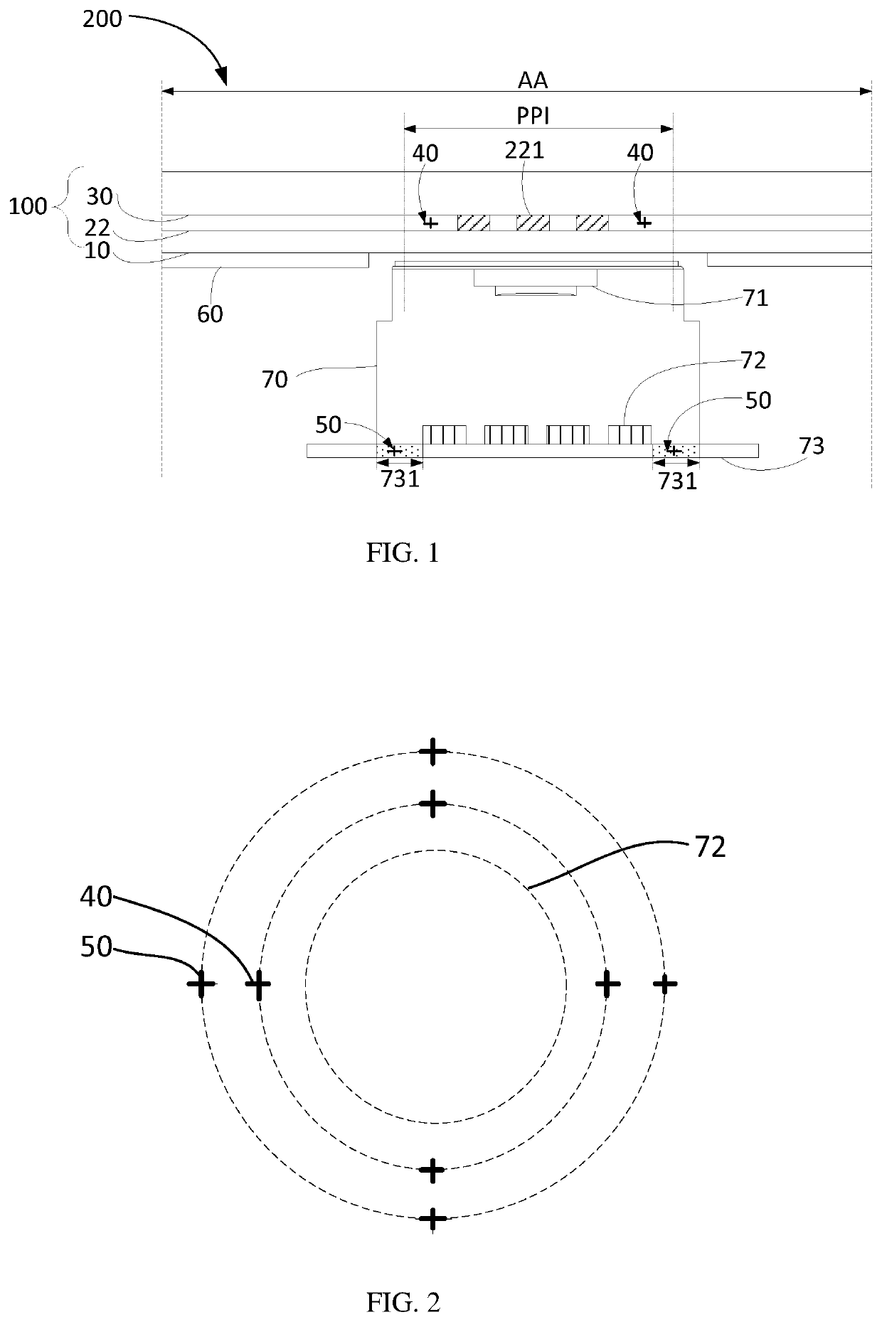
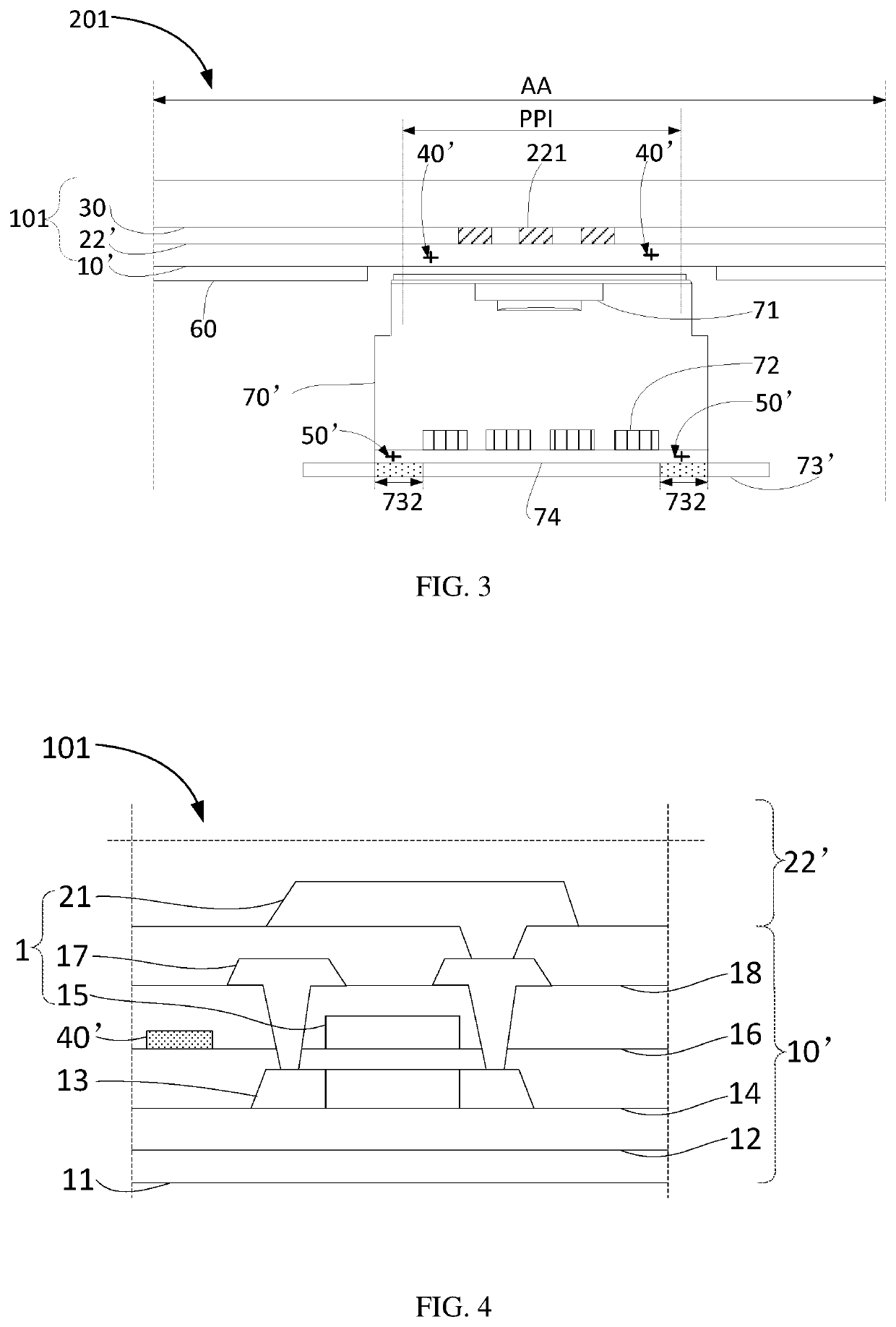
[0035]Referring to FIG. 1, in one embodiment, an organic light emitting diode (OLED) display device 200 includes:

[0036]a display panel 100, and the display panel 100 is provided with a low pixel density area (PPI);

[0037]an attachment component 60 attached to a backside of the display panel 100, and an area of the attachment component corresponding to the low pixel density area is hollowed out; and

[0038]a camera 70 disposed on the backside of the display panel 100 and corresponding to the low pixel density area (PPI). A first alignment mark 40 is disposed in the low pixel density area (PPI) of the display panel 100, and a second alignment mark 50 is disposed inside the camera, and arrangements of the first alignment mark 40 and the second alignment mark 50 are consistent.

[0039]In one embodiment, the low pixel density area (PPI) ma...


PUM

PropertyMeasurementUnit
pixel densityaaaaaaaaaa
photosensitiveaaaaaaaaaa
areaaaaaaaaaaa

Abstract

An organic light emitting diode (OLED) display device is provided. The OLED display device includes a display panel and a camera. A first alignment mark is formed on a low pixel density area of the display panel, a second alignment mark is formed in the camera, and arrangements of the first alignment mark and the second alignment mark are consistent. Therefore, an alignment accuracy between the camera and the display panel is improved, and a purpose of adopting a blind hole in the area where the camera is mounted on the display device and displaying normally is achieved.

Description

CROSS REFERENCE[0001]The present application claims priority to Chinese Patent Application No. 201910821922.1, filed on Sep. 2, 2019, filed for the invention titled “Organic light emitting diode display device and method of manufacturing thereof,” which is hereby incorporated by reference in its entirety.BACKGROUND OF INVENTIONField of Invention[0002]The present invention relates to the field of display technology, and more particularly, to an organic light emitting diode display device and a method of manufacturing thereof.Description of Prior Art[0003]Active-matrix organic light emitting diode (AMOLED) full screens are relatively popular products. Enlarging a screen ratio may improve user experience. In order to achieve a high screen ratio, expanding a display area is achieved by adopting under-screen devices. Accordingly, all modules such as front camera, receiver, and fingerprint recognition of the mobile phone are disposed on a backside of the display screen.[0004]In a currentl...

Claims


Application Information

Patent Timeline
Patent Type & Authority Patents(United States)
IPC IPC(8): H01L29/08H01L25/18H01L25/00H01L27/146H01L27/32H05K1/02H01L27/148H05K1/18
CPCH01L25/18H01L25/50H01L27/14618H01L27/3272H05K1/0269H01L27/14643H01L27/14806H05K1/18H05K2201/10121H05K2201/10128H10K59/65H10K59/12H04M1/0264H04M1/0266H05K2201/09918H05K2203/166H05K3/303H01L23/552H10K59/126
Inventor ZHAN, DONG
Owner WUHAN CHINA STAR OPTOELECTRONICS SEMICON DISPLAY TECH CO LTD
Why Eureka
Try Eureka