Electronic device and fabrication method of the same

a technology of electronic devices and fabrication methods, applied in the field of electronic devices, can solve the problems of increased production costs and reduced yield

Active Publication Date: 2022-10-25
AU OPTRONICS CORP
View PDF12 Cites 0 Cited by
  • Summary
  • Abstract
  • Description
  • Claims
  • Application Information

AI Technical Summary

Benefits of technology

[0026]According to the foregoing embodiments, through the design of the laminated structures at the side containing arrays, the projection of the protection layer on the second substrate can be spaced apart from the transmission region TR. In addition, the alignment film can be conformally formed on the protection layer, the buffer layer, and the second substrate, thereby increasing the light transmittance of the transmission region and reducing the difference of the light transmittance. In addition, since there is no need to form the transmission region TR by drilling process, the process of forming the transmission region may be integrated with the process of forming the panel. Therefore, the fabrication cost may be reduced and the yield may be increased.

Problems solved by technology

However, this method requires glass drilling process and sealing process around the holes.
As a result, the fabrication cost is increased and the yield is decreased.

Method used


Image

  • Electronic device and fabrication method of the same
  • Electronic device and fabrication method of the same
  • Electronic device and fabrication method of the same

Examples


Embodiment Construction

[0043]Reference will now be made in detail to the present embodiments of the disclosure, examples of which are illustrated in the accompanying drawings. Wherever possible, the same reference numbers are used in the drawings and the description to refer to the same or like parts.

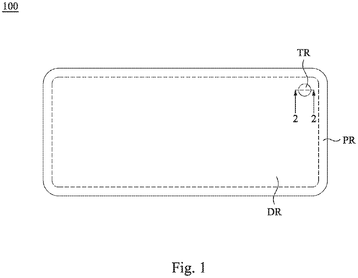
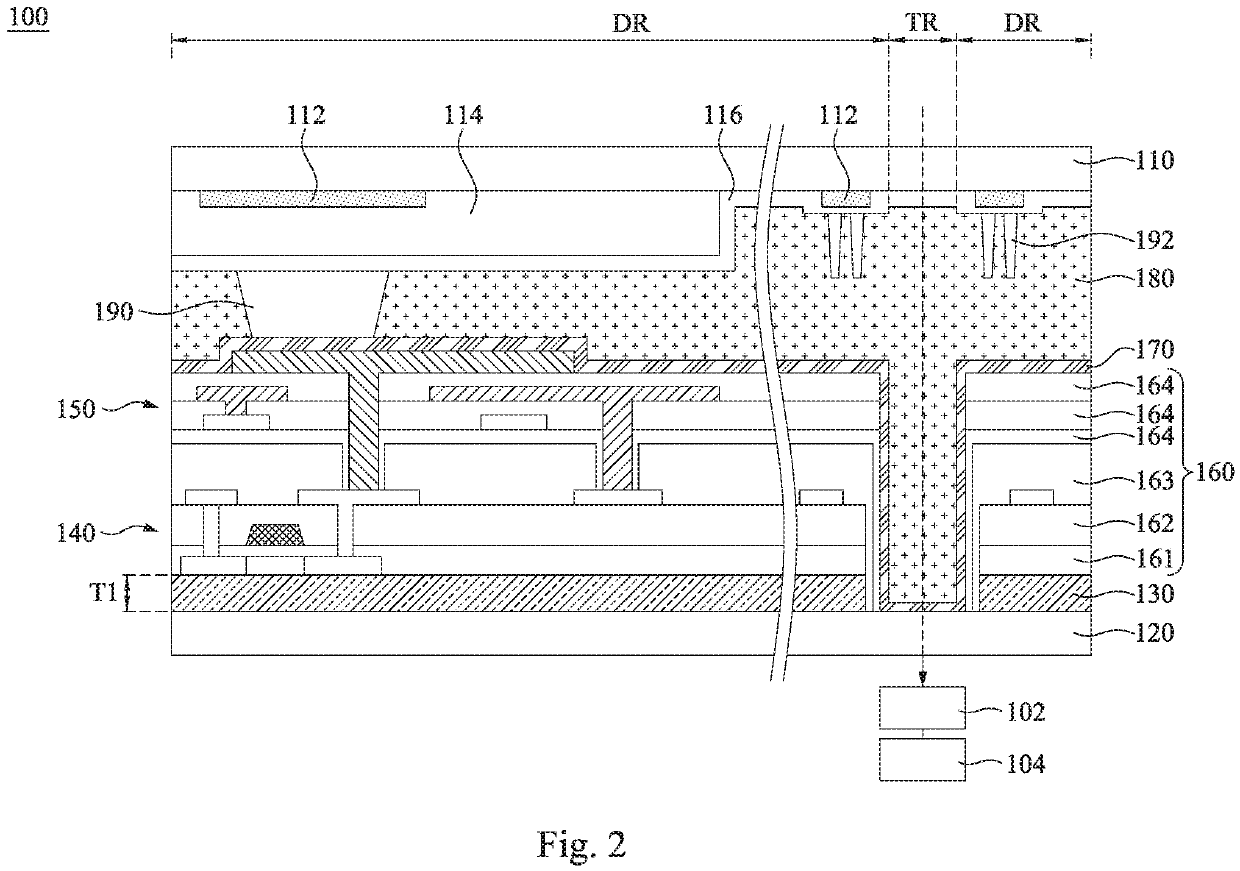
[0044]FIG. 1 is a top view of an electronic device 100 according to one embodiment of the present disclosure. FIG. 2 is a cross-sectional view taken along line 2-2 in FIG. 1. Reference is made to FIG. 1 and FIG. 2 simultaneously. The electronic device 100 includes a first substrate 110, a second substrate 120, a buffer layer 130, a pixel array 150, an active array 140, a protection layer 160, and an alignment film 170. The first substrate 110 includes a periphery region PR, a display region DR, and a transmitting region TR. The periphery region PR surrounds the display region DR, and the display region DR surrounds the transmission region TR. For clarity and simplicity, only the display region DR and the tran...


PUM

PropertyMeasurementUnit
thicknessaaaaaaaaaa
thicknessaaaaaaaaaa
thicknessaaaaaaaaaa

Abstract

An electronic device includes a first substrate, a second substrate, a buffer layer, an active array, a pixel array, a protection layer and an alignment film. The first substrate includes a transmission region, a display region, and a periphery region. The periphery region surrounds the display region, and the display region surrounds the transmission region. The first substrate is disposed opposite to the second substrate. The buffer layer is disposed on the second substrate. The protection layer is disposed on the buffer layer, and a projection of the protection layer on the second substrate is apart from the transmission region. The active array is disposed on the buffer layer. The pixel array is disposed on the active array and is electrically connected to the active array. The alignment film is conformally disposed on the protection layer, the buffer layer, and the second substrate.

Description

RELATED APPLICATIONS[0001]This application claims priority to Taiwan Application Serial Number 108127046, filed Jul. 30, 2019, and Taiwan Application Serial Number 109100652, filed Jan. 8, 2020, which are herein incorporated by references.BACKGROUNDTechnical Field[0002]The present disclosure relates to an electronic device.Description of Related Art[0003]High screen-to-body ratio has been a standard of the mobile phone nowadays except for power saving and high quality. Therefore, how to reduce the area occupied by other functions has been a developing direction for increasing the screen-to-body ratio. For example, regarding the holes for depositing the front camera and the sensor, the available method is to drill a hole such that the front camera and the sensor can be put into the hole. However, this method requires glass drilling process and sealing process around the holes. As a result, the fabrication cost is increased and the yield is decreased.SUMMARY[0004]One aspect of the pre...

Claims


Application Information

Patent Timeline
Patent Type & Authority Patents(United States)
IPC IPC(8): G02F1/1362G02F1/1335G02F1/1333G03B29/00G03B30/00
CPCG02F1/136213G02F1/133512G02F1/133388G02F1/1333G02F1/1337G03B29/00G02F1/13318
Inventor SU, CHIH-CHUNGCHEN, YI-WEI
Owner AU OPTRONICS CORP
Why Eureka
Try Eureka