Apparatus and method for manufacturing a semiconductor package

a semiconductor and packaging technology, applied in the field of apparatus and method for manufacturing flipchip semiconductor packages, can solve the problems of reducing difficulty in completely filling the gap between the semiconductor reducing the rate at which the resin enters the gap between the chip and the mount board, so as to improve the grade and quality of the semiconductor devi

Inactive Publication Date: 2001-05-03
KK TOSHIBA
View PDF0 Cites 7 Cited by
  • Summary
  • Abstract
  • Description
  • Claims
  • Application Information

AI Technical Summary

Benefits of technology

6. In view of these problems, it is an object of the present invention to remove the above-mentioned drawbacks and to provide an apparatus and method for m...

Problems solved by technology

However, the rate at which the resin enters the gap between the chip and mount board is typically lower than the rate at which the resin advances around the periphery of the semiconductor chip.
Thus, using the conventional method in which the resin is uniformly supplied by a syringe driven at a constant speed, it is difficult to complete...

Method used


Image

  • Apparatus and method for manufacturing a semiconductor package
  • Apparatus and method for manufacturing a semiconductor package
  • Apparatus and method for manufacturing a semiconductor package

Examples


first embodiment

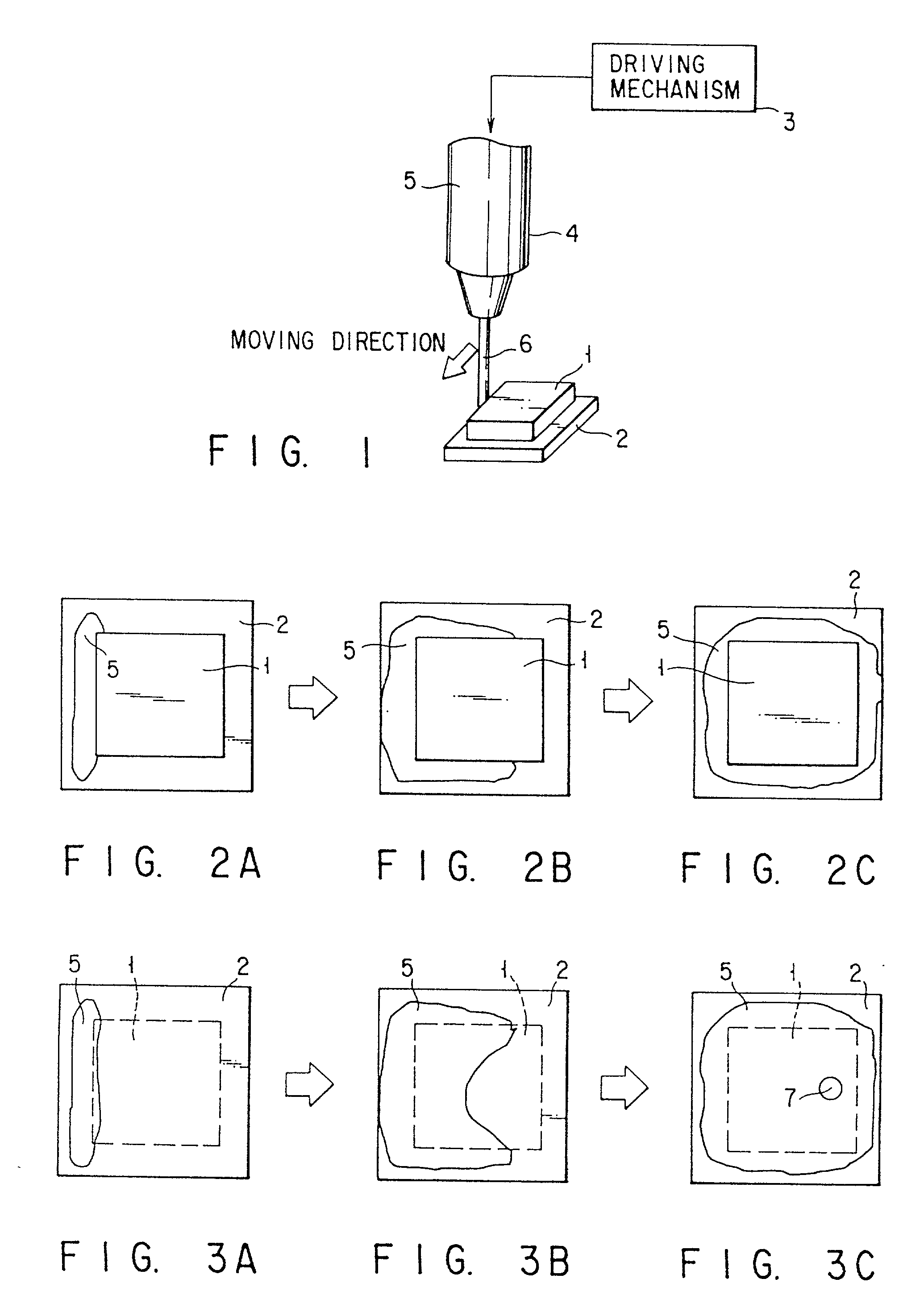
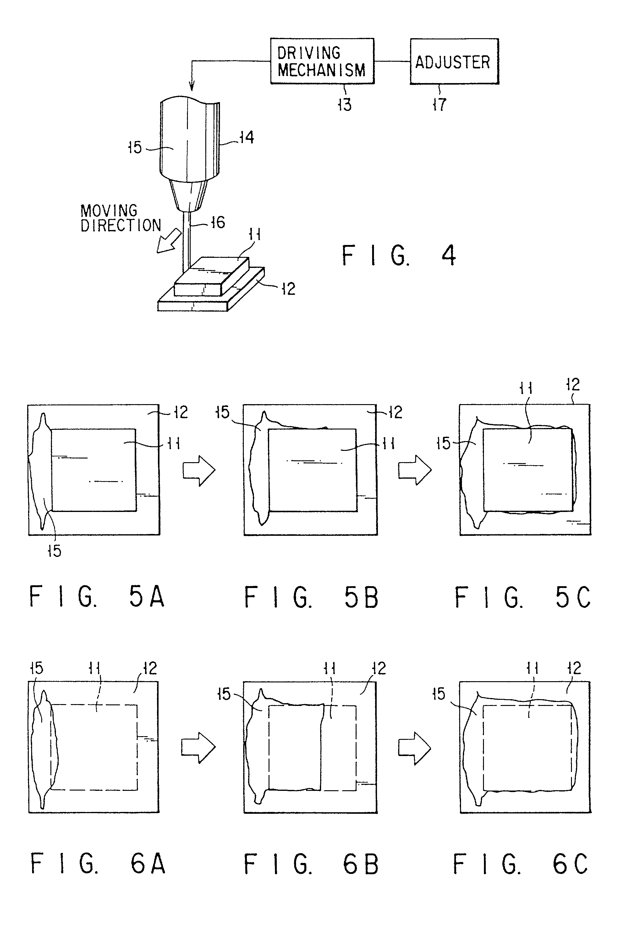
23. FIG. 4 shows a method for manufacturing a semiconductor package according to the present invention. A semiconductor chip 11 is mounted on a mount board 12 by a flip-chip connection, and then a driving mechanism 13 moves a syringe 14 along one side of the semiconductor chip (in the direction indicated by the arrow in the figure). In more detail, the semiconductor chip 11 is provided with electrode pads that are arranged along the periphery of the chip. Wiring pads are arranged on the surface of the mount board 12 at positions corresponding to the electrode pads of the semiconductor chip 11, and are connected to the electrode pads via metal bumps (e.g., solder bumps). The wiring pads are led out of the bottom surface of the mount board 12 via through-holes and are connected to external pads that are arranged, for example, in a matrix on the reverse surface of the mount board. The mount board is typically formed with materials such as epoxy resin, alumina (Al.sub.2O.sub.3), aluminu...

fifth embodiment

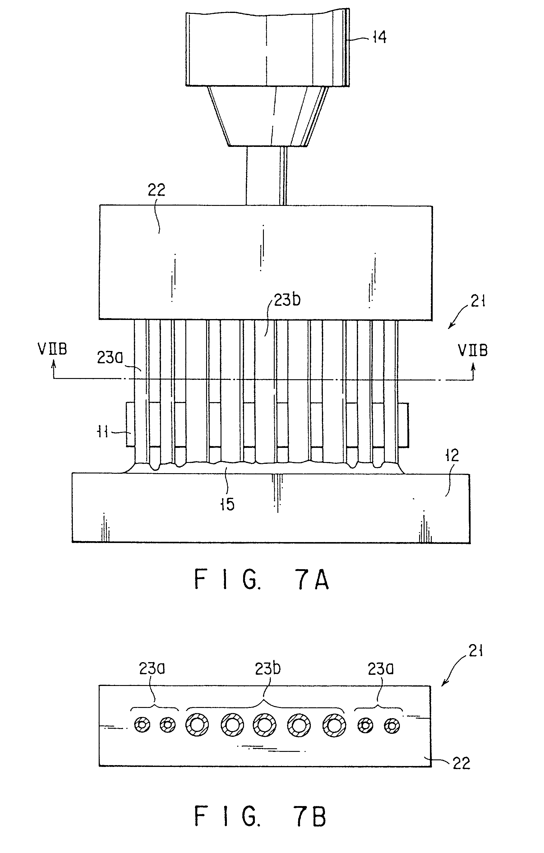
36. Similar to the fifth embodiment, the viscosity of the resin flowing through the gap is partially varied by controlling the temperature distribution of the mount board so that the portions of the mount board corresponding to the end portions of the semiconductor chip are at a lower temperature than the portion of the mount board corresponding to a central portion of the chip. Thus, as the resin is supplied to the mount board (e.g., by a multi-nozzle 65 having a nozzle support body 63 and nozzles 64 with the same diameter), the viscosity of the resin near the central portion of the chip is reduced so that the rate at which the resin flows through the gap near the central portion of the chip is higher than the rate at which the resin flows near the peripheral portions of the chip (see equations 1 and 2). Accordingly, the heater block and adjacent radiator plates allow the resin to completely fill the gap so that a high-grade, high-quality semiconductor device is produced.

37. In the...


PUM

PropertyMeasurementUnit
Temperatureaaaaaaaaaa
Diameteraaaaaaaaaa
Speedaaaaaaaaaa

Abstract

An apparatus is provided for manufacturing a semiconductor package of the type in which a gap between a semiconductor chip and a mount board is filled with a resin. The apparatus includes resin supply means for supplying the resin along one side of the semiconductor chip, and resin supply control means for controlling the amount of resin supplied by the resin supply means such that more resin is supplied near the central portion of the semiconductor chip than near the end portions of the semiconductor chip. Also provided is a method that includes the steps of connecting the semiconductor chip and the mount board, and supplying the resin along one side of the semiconductor chip in such a manner that more resin is supplied near a central portion of the semiconductor chip than near the end portions of the semiconductor chip. According to the present invention, the resin is supplied such that it is relatively less concentrated near the peripheral portions of the chip so the resin spreads throughout the entire gap at substantially the same time as it flows along the peripheral portion of the chip. Thus, the formation of resin-less voids in the gap is deterred so that the grade and quality of the semiconductor device is improved.

Description

BACKGROUND OF THE INVENTION1. This invention relates to an apparatus and method for manufacturing a flip-chip-type semiconductor package, and more specifically to an apparatus and method for manufacturing a semiconductor package in which formation of a resin-less void in the gap between the semiconductor chip and a mount board is suppressed, so that the grade and quality of the semiconductor device is improved.2. There has recently been developed a "flip-chip" method for packaging semiconductor chips. The flip-chip method produces a small semiconductor package in which a semiconductor chip is bonded to a mount board. Typically, solder bumps are formed on the electrode pads of the semiconductor chip, and the solder bumps are connected to the pads and wiring of the mount board. A resin is filled in a gap between the semiconductor chip and the mount board to secure the package. FIG. 1 shows a conventional method for fabricating a semiconductor package that has a semiconductor chip and ...

Claims


Application Information

Patent Timeline
IPC IPC(8): B05B1/14B05B13/04B05C5/00B05C5/02B05C9/14H01L21/00
CPCB05B1/14B05B13/04B05C5/001B05C5/0208B05C9/14H01L21/6715Y10T29/53174Y10T156/1798Y10T29/4913H01L24/743H01L2224/16225H01L2224/32225H01L2224/73204H01L2224/92125H01L2924/00
Inventor NAKAZAWA, TAKAHITONOMURA, HIROSHIOHSHIMA, YUMIKO
Owner KK TOSHIBA
Why Eureka
Try Eureka