Semiconductor package and manufacturing method thereof

a technology of semiconductor and manufacturing method, applied in the direction of semiconductor/solid-state device details, semiconductor devices, electrical apparatus, etc., can solve the problems of relatively expensive circuit board 10, relatively complicated manufacturing procedure, and disadvantages of conventional semiconductor packages constructed as mentioned abov

Inactive Publication Date: 2001-06-21
AMKOR TECH INC DW US
View PDF0 Cites 28 Cited by
  • Summary
  • Abstract
  • Description
  • Claims
  • Application Information

AI Technical Summary

Problems solved by technology

However, the conventional semiconductor package constructed as mentioned above has disadvantages.
For example, circuit board 10 is relatively expensive to make, since the stepped portion and internal cavity must be formed to allow the semiconductor chip and glass p

Method used


Image

  • Semiconductor package and manufacturing method thereof
  • Semiconductor package and manufacturing method thereof
  • Semiconductor package and manufacturing method thereof

Examples


Embodiment Construction

[0036] Exemplary embodiments of the present invention are illustrated in the accompanying drawings. Wherever possible, the same reference numerals will be used throughout the drawings and the description to refer to the same or like parts.

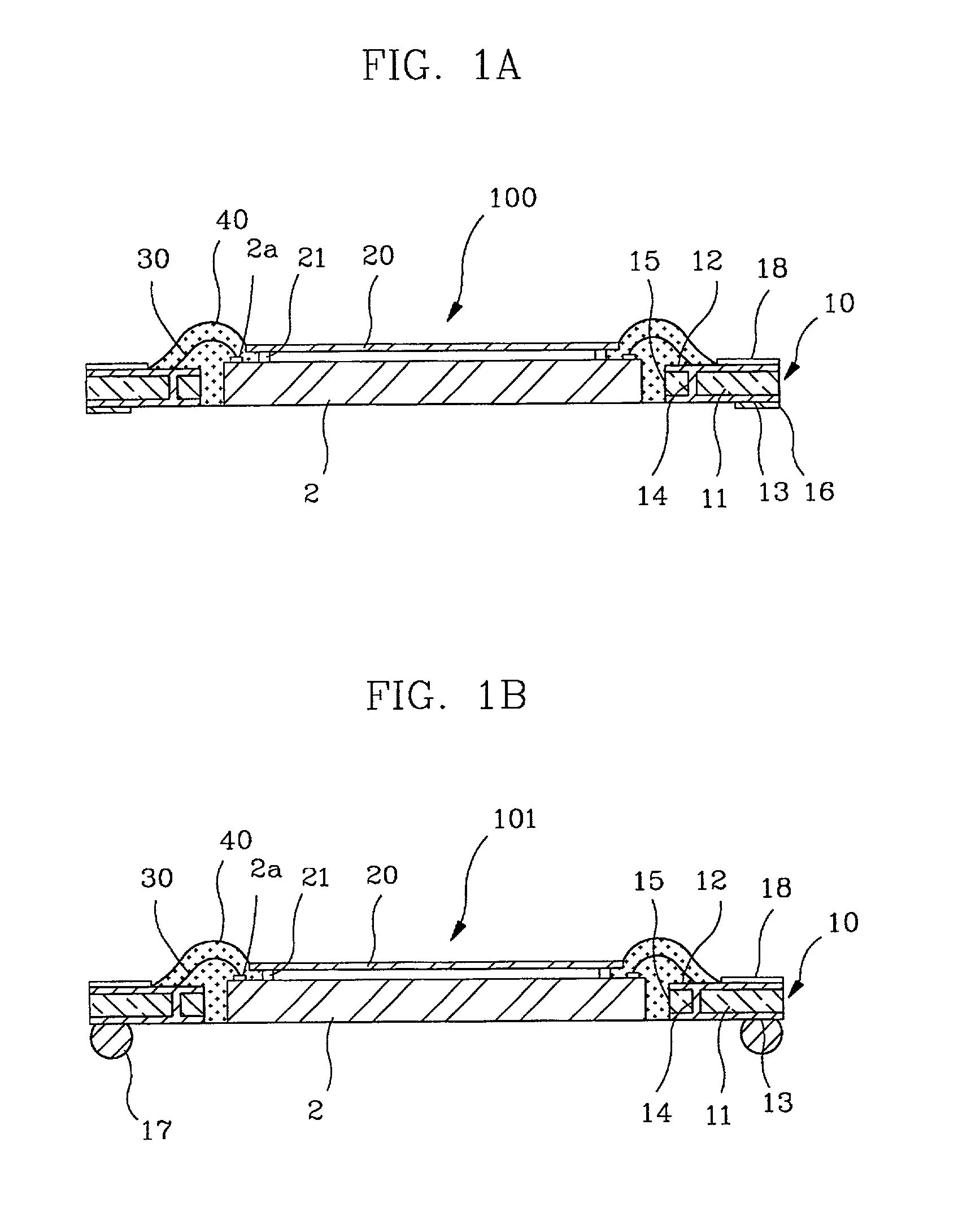
[0037] FIGS. 1A and 1B are cross-sectional side views respectively illustrating semiconductor packages 100 and 101 in accordance with first and second embodiments of the present invention.

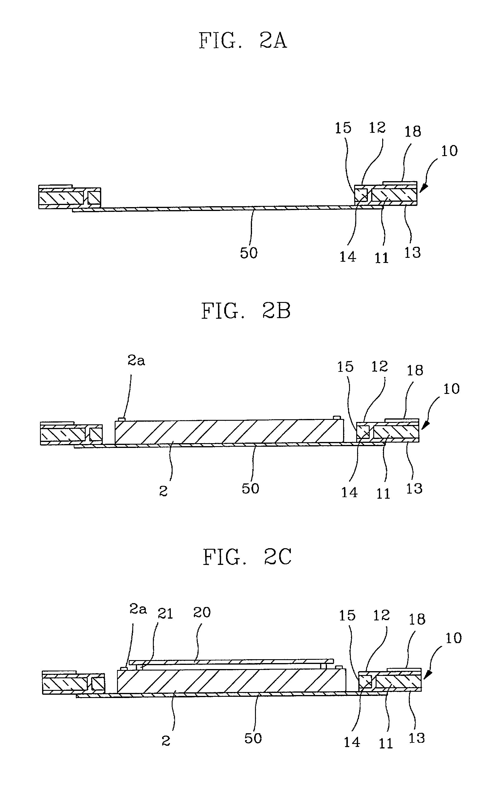
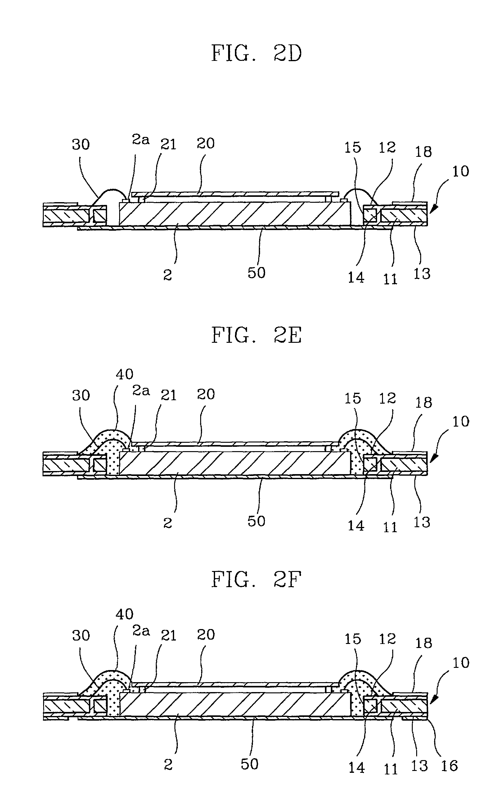
[0038] First, a CCD or other optical semiconductor chip 2 is provided that has input and output pads 2a formed on an active upper surface thereof. A transparent plate 20 formed of optically clear glass, plastic, quartz or the like is positioned over and transmits light to (or from) the upper surface of the semiconductor chip 2, and is supported thereon by a dam 21. In this example, a glass plate 20 is used. Glass plate 20 enables the semiconductor chip 2 to easily receive light from an external source.

[0039] In this example, a double-sided ring of adhesive tape or...


PUM


Abstract

Embodiments of a semiconductor package and manufacturing methods therefor are disclose. An exemplary package comprises an optical semiconductor chip having input and output pads on an upper surface thereof. A transparent plate is bonded to the chip via a dam located within the input and output pads. The chip is mounted within an aperture through a planar circuit board. Wires electrically connect the input and output pads to circuit patterns of the circuit board. An encapsulant fills the aperture, and supports the chip therein. Interconnects are formed on the lower surface of the circuit board. An alternative embodiment omits the dam and the wires and employs a flip chip style connection between the chip and circuit patterns on the transparent plate. The transparent is supported by and attached to the upper surface of the planar circuit board.

Description

[0001] 1. Field of the Invention[0002] The present invention relates to a semiconductor package and a manufacturing method thereof, and more particularly, the present invention relates to a semiconductor package for an optical semiconductor chip and a manufacturing method for the package.[0003] 2. Description of the Related Art[0004] Semiconductor packages are sometimes made to allow the transmission of light to or from an optical semiconductor chip mounted within the package. One type of optical semiconductor chip is a charge coupled device, or CCD. A CCD is used, for example, in an image signaling system of a television camera.[0005] In a television camera, external light passes through lenses. Thereafter, the light is separated into three primary colors by a color separating optical system. The three primary colors are provided on, and form an image on, a light receiving active surface of the CCD. The CCD electronically scans the image to convert the image into an electrical sign...

Claims


Application Information

Patent Timeline
IPC IPC(8): H01L23/28H01L21/00H01L21/44H01L21/48H01L21/56H01L23/12H01L29/768H01L31/113
CPCH01L27/14618H01L27/14687H01L2224/32225H01L2224/48091H01L2224/48227H01L2224/73265H01L2224/85001H01L2224/8592H01L2924/01046H01L2924/01079H01L2924/15153H01L2924/15165H01L2924/15311H01L2924/16195H01L2924/18165H01L2924/00014H01L2224/45144H01L2224/45124H01L2924/00H01L2924/16235
Inventor PARK, YOUNG KUKMOON, DOO HWANHA, SUN HOHAN, CHANG SUK
Owner AMKOR TECH INC DW US
Why Eureka
Try Eureka