Method for making an insulating film

a technology of insulating film and film layer, which is applied in the direction of semiconductor devices, semiconductor/solid-state device details, electrical equipment, etc., can solve problems such as metal wiring corrosion

Inactive Publication Date: 2001-11-08
SONY CORP
View PDF0 Cites 12 Cited by
  • Summary
  • Abstract
  • Description
  • Claims
  • Application Information

AI Technical Summary

Benefits of technology

0007] It is therefore an object of the invention to provide a method for making an insulating film free from problems s

Problems solved by technology

Under the condition, if the inter-layer insulating film underlying the SiO.sub.2 film contains H.sub.2O and has a fluidity, then NH.sub.3 produced in vapor is incorporated (absorbed) into the underlying inter-layer insulating film. NH.sub.3

Method used


Image

  • Method for making an insulating film
  • Method for making an insulating film
  • Method for making an insulating film

Examples


first embodiment

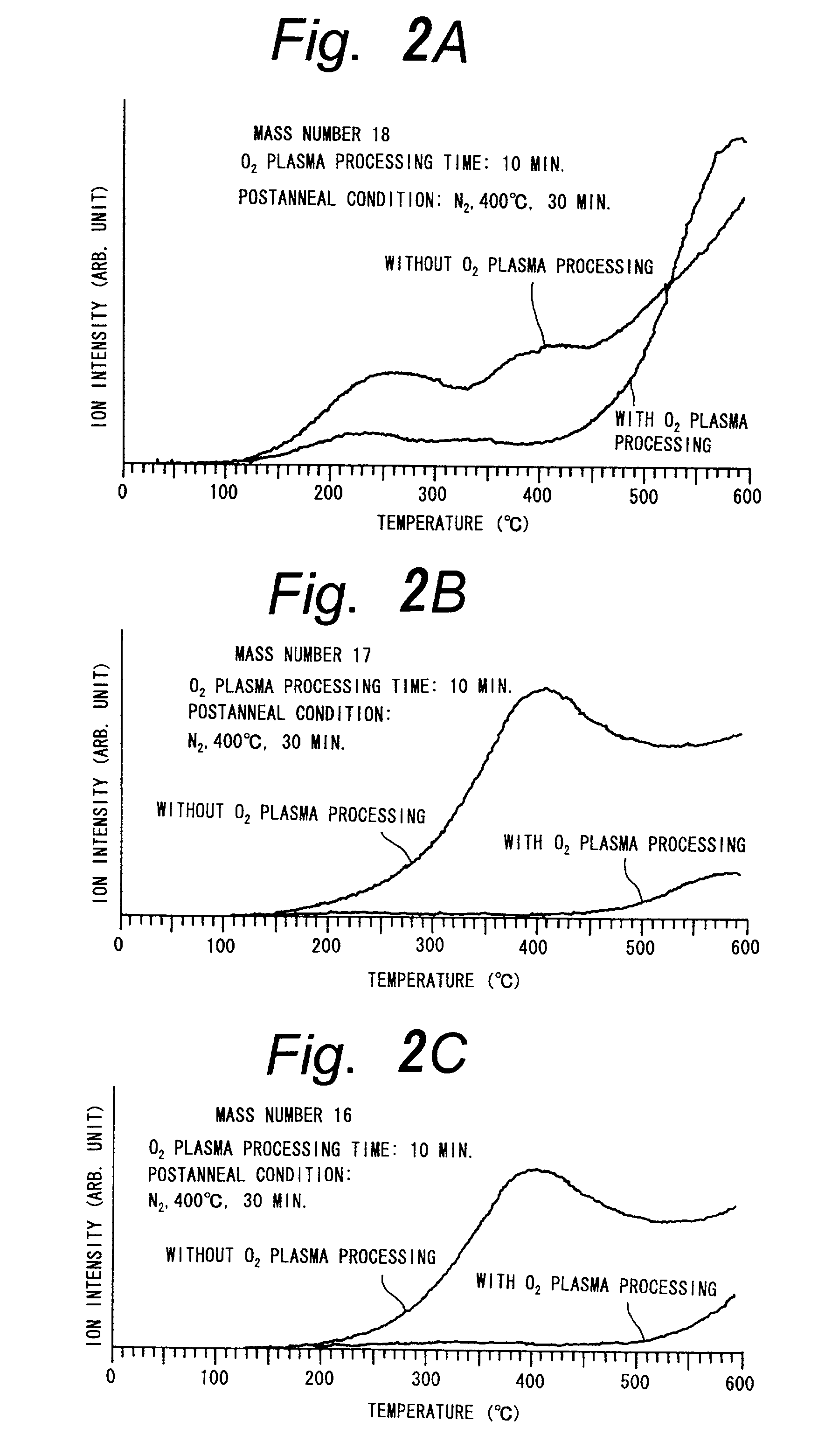
[0051] As explained above, substantially all H.sub.2O can be removed from the surface of the inter-layer insulating film 4 by treating the inter-layer insulating film 4 by O.sub.2 plasma processing after making the inter-layer insulating film 4 as a fluid film. Therefore, even when the SiO.sub.2 film 5 is made as a cap layer directly on the inter-layer insulating film 4 by plasma CVD, NH.sub.3 produced in vapor by plasma during the process is never incorporated into the inter-layer insulating film 4. As a result, corrosion of the Al alloy wiring 2 or the problem of poisoned via do not occur.

second embodiment

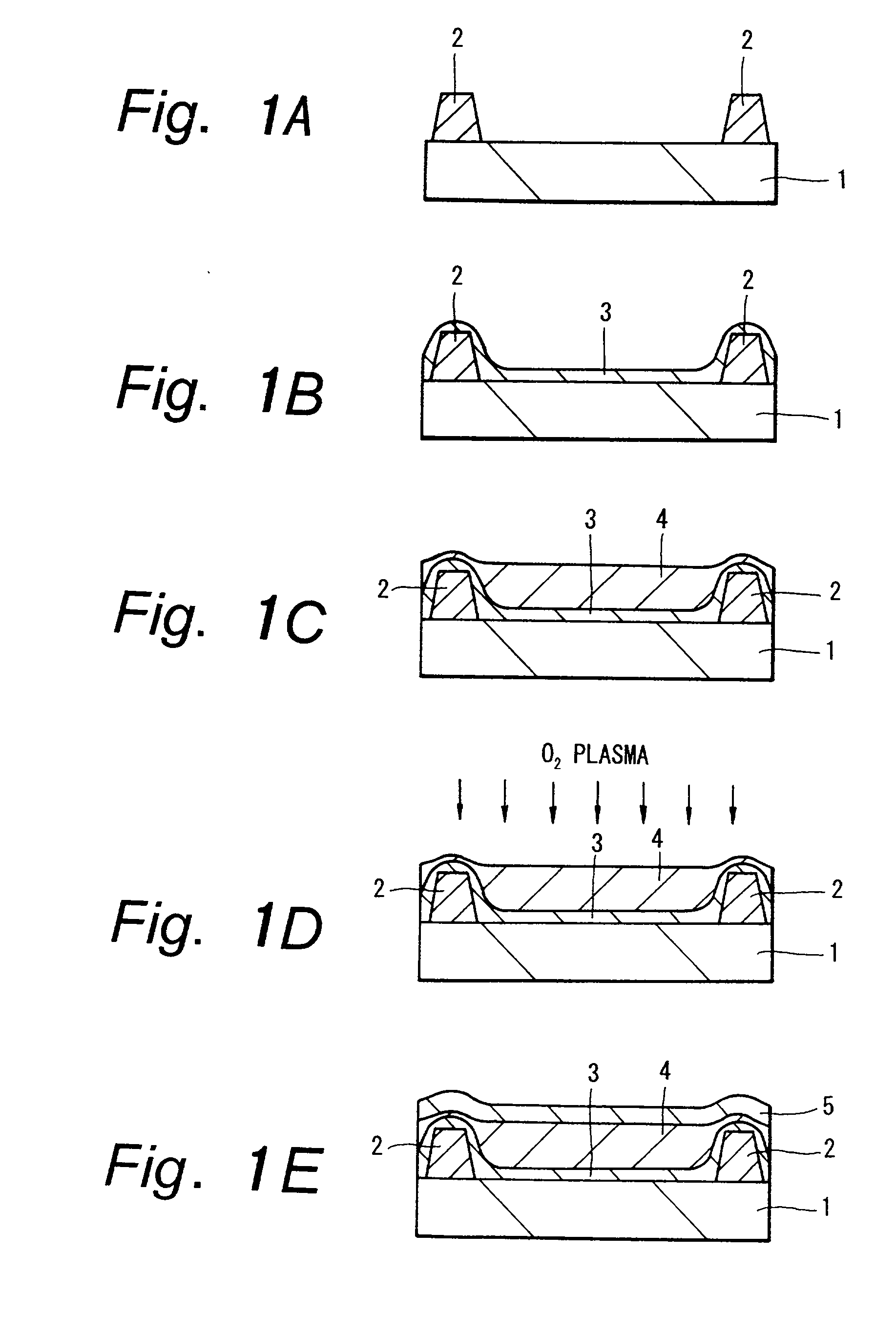
[0052] FIGS. 3A through 3E show a method for making an inter-layer insulating film according to the invention.

[0053] In the embodiment shown here, the Al alloy wiring 2 is formed on the Si substrate 1 having formed a device and covered with an inter-layer insulating film previously as shown in FIG. 3A,.

[0054] Next, as shown in FIG. 3B, a non-fluid SiO.sub.2 film 3 is made as a base layer on the Si substrate 1 by plasma CVD using SiH.sub.4 and N.sub.2O, for example, as source materials.

[0055] Next, as shown in FIG. 3C, a fluid inter-layer insulating film 4 is made by low pressure CVD using Si(CH.sub.3)H.sub.3 and H.sub.2O.sub.2, for example, as source materials. The steps heretofore are the same as those of the first embodiment.

[0056] Next, as shown in FIG. 3D, the surface of the inter-layer insulating film 4 is heated by lamp heating, namely by using radiant heat from a lamp heater, to cure the surface of the inter-layer insulating film 4 by rapid thermal annealing in a short time. ...

third embodiment

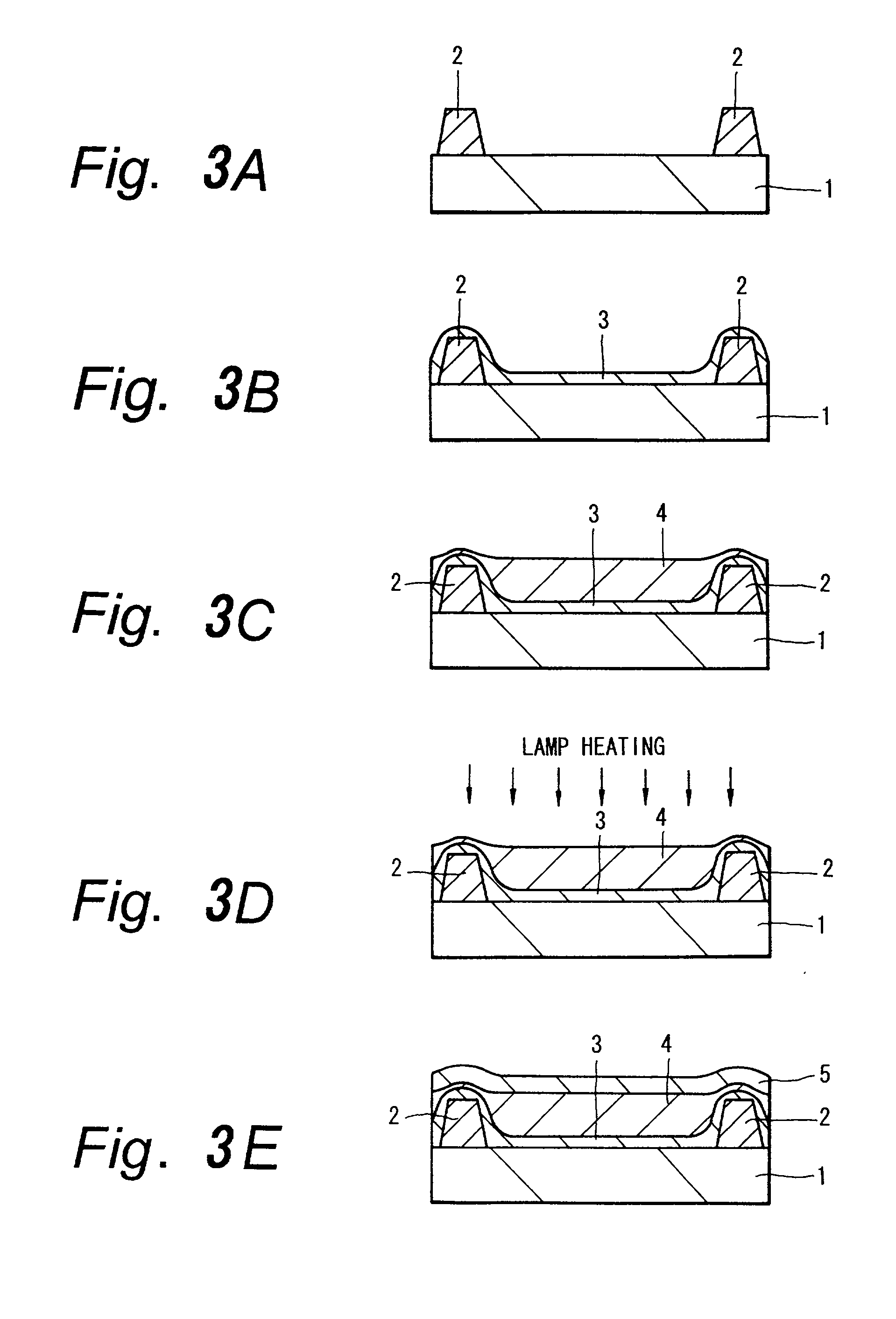
[0068] FIGS. 4A through 4E show a method for making an inter-layer insulating film according to the invention.

[0069] In the embodiment shown here, the Al alloy wiring 2 is formed on the Si substrate 1 having formed a device and covered with an inter-layer insulating film previously as shown in FIG. 4A.

[0070] Next, as shown in FIG. 4B, a non-fluid SiO.sub.2 film 3 is made as a base layer on the Si substrate 1 by plasma CVD using SiH.sub.4 and N.sub.2O, for example, as source materials.

[0071] Next, as shown in FIG. 4C, a fluid inter-layer insulating film 4 is made by low pressure CVD using Si(CH.sub.3)H.sub.3 and H.sub.2O.sub.2, for example, as source materials. The steps heretofore are the same as those of the first embodiment.

[0072] Next, as shown in FIG. 4D, the Si substrate 1 is set in a chamber 6 and heated while introducing O.sub.3 into the chamber to cure the surface of the inter-layer insulating film 4 by O.sub.3 annealing of the inter-layer insulating film 4. By the O.sub.3 a...


PUM


Abstract

In a method for manufacturing an insulating film using a fluid source material without inviting corrosion of metal wiring or the problem of poisoned via, after making a SiO2 film as a base layer on an Si substrate defining an uneven surface with an Al alloy wiring by plasma CVD using SiH4 and N2O, and further making an inter-layer insualting film having a fluidity on the SiO2 film by low pressure CVD using SiH4 or organosilane and H2O2, O2 plasma processing is applied to the inter-layer insulating film. After that, a SiO2 film as a cap layer is made on the inter-layer insulating film by plasma CVD using SiH4 and N2O. Rapid thermal annealing using lamp heating or O3 annealing may be done in lieu of O2 plasma processing.

Description

[0001] 1. Field of the Invention[0002] This invention relates to a method for making an insulating film particularly suitable for use in making an inter-layer insulating film in a semiconductor device.[0003] 2. Description of the Related Art[0004] In a process of manufacturing a semiconductor device, a method for making an inter-layer insulating film using a fluid source material is often used to level the surface of a substrate by smoothing unevenness made by wiring or the like. Such an inter-layer insulating film contains much moisture (H.sub.2O) and is highly fluid.[0005] In conventional techniques, a non-fluid cap layer was formed directly on a fluid inter-layer insulating film containing much H.sub.2O by plasma CVD (for example, 1995 Dry Process Symposium, pp.261-268) to prevent cracks in the fluid inter-layer insulating film containing H.sub.2O during post-annealing. Typically used as the cap layer was a SiO.sub.2 film made of SiH.sub.4 and N.sub.2O by plasma CVD because N.sub...

Claims


Application Information

Patent Timeline
IPC IPC(8): H01L21/316H01L21/768H01L23/522
CPCH01L21/76801H01L21/76826H01L21/76828H01L21/76834H01L21/31
Inventor HARA, MASAKI
Owner SONY CORP
Why Eureka
Try Eureka