
Spacing violation checker

a technology of spacing violation and checker, which is applied in the direction of computer aided design, program control, instruments, etc., can solve the problems of affecting the final physical design layout of the ineffectiveness of simple gridded solutions with today's current wide wires, and the inability to correct the minimum spacing violation after the final physical design layout is complete,

Inactive Publication Date: 2001-11-15
GLOBALFOUNDRIES INC
View PDF1 Cites 19 Cited by
  • Summary
  • Abstract
  • Description
  • Claims
  • Application Information

AI Technical Summary

Benefits of technology

[0011] The invention is superior to conventional systems because the invention allows same net spacing errors to be recognized during physical design prior to Design Rules Check. The software supporting the invention performs orders of magnitude faster than the Design Rules Check solution. As such, the invention dramatically decreases the turn-around time of physical design, providing a fast solution which is available prior to final layout release.

Problems solved by technology

Therefore, a simple gridded solution is no longer effective with today's current wide wires.
Design Rules Check is an expensive and time consuming process which is usually run after the final physical design layout is complete.
Further, correcting minimum spacing violations after the final physical design layout is complete is also a difficult and expensive process.

Method used


Image

  • Spacing violation checker
  • Spacing violation checker
  • Spacing violation checker

Examples


Embodiment Construction

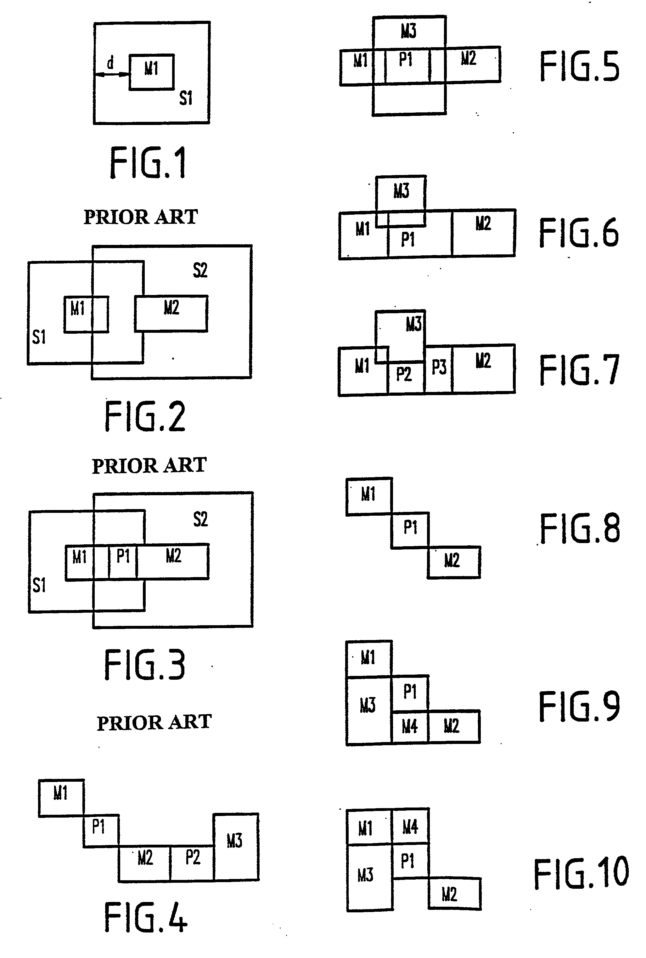
[0025] Referring now to the drawings, and more particularly to FIG. 1, a rectangle representing a conductor shape M1, such as a metal wiring, and a spacing rectangle S1, which defines a minimum space "d" according to design rules around the metal shape M1 are illustrated. The metal shape is a part of a larger overall conductive net within a structure, such as a semiconductor. The metal shape comprises circuit components which operate by transmission of signals through the net.

[0026] A first stage of the invention involves a plane sweep of all the net's components (e.g., net parts) such as vias, wires segments, pins or powers. The first rectangle M1 represents the shape of the net part and the second rectangle S1 represents the minimum spacing requirement surrounding the net part M1. The size of the second minimum spacing rectangle S1 is determined by the design rules for net part M1 such as the minimum space "d", as mentioned above. While the minimum spacing rectangles S1 are illust...


PUM


Abstract

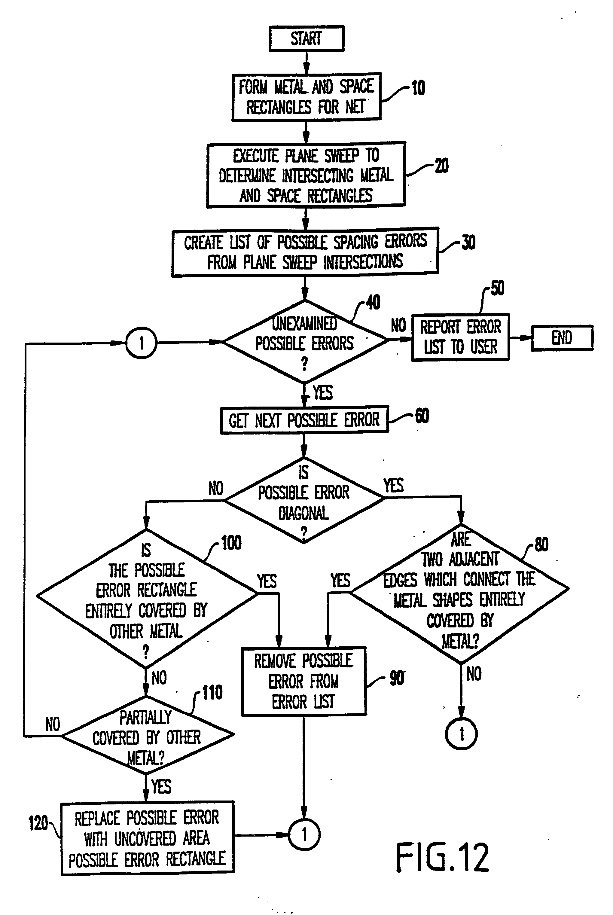
A structure and method for testing spacing of wiring in a circuit comprises forming a plurality of conductor rectangles representative of conductors of the circuit, forming minimum spacing rectangles around the conductor rectangles (the minimum spacing rectangles being larger than respective ones of the conductor rectangles), identifying a possible error rectangle when a first conductor rectangle of the conductor rectangles occupies a portion of a minimum spacing rectangle of a second conductor rectangle of the conductor rectangles, checking whether the possible error rectangle is a true error, and reporting the true errors.

Description

[0001] 1. Field of the Invention[0002] The present invention generally relates to methods and systems for checking spacing of wiring in a semiconductor structure and more particularly to a method and system for checking the spacing of wiring within a single net.[0003] 2. Description of the Related Art[0004] Conventional design rules require wires of the same net within a semiconductor structure to be spaced a specified minimum distance apart. Older designs satisfied the minimum spacing requirements fairly easily through simplified grid designs which automatically guaranteed that minimum spacing design rules were met. However, with advancing technologies wider wires are more prevalent. Such wide wires have larger spacing requirements than the older narrower wires. Therefore, a simple gridded solution is no longer effective with today's current wide wires.[0005] Minimum spacing violations were conventionally recognized during the shapes processing performed by Design Rules Check (DRC)...

Claims


Application Information

Patent Timeline
Patent Type & Authority Applications(United States)
IPC IPC(8): G06F17/50
CPCG06F17/5081G06F30/398
Inventor DARDEN, LAURA R.
Owner GLOBALFOUNDRIES INC
Learn More