Semiconductor device

Active Publication Date: 2007-03-13
RENESAS ELECTRONICS CORP
View PDF6 Cites 27 Cited by
  • Summary
  • Abstract
  • Description
  • Claims
  • Application Information

AI Technical Summary

Benefits of technology

[0037]When performing the read operation and the verify read operation during the write operation in parallel in different hierarchies, the p

Problems solved by technology

The above hierarchal bit line structure only with main and sub-bit lines cannot solve signal propagation delay due to the main bit line load capacity and cannot cope with the desire to increase the read speed.
Each of the arrays must be provided with a read circuit, a write circuit and an interface circuit with the bus line corresponding to the number of the divided arrays, resulting in increased size of

Method used


Image

  • Semiconductor device
  • Semiconductor device
  • Semiconductor device

Examples


Embodiment Construction
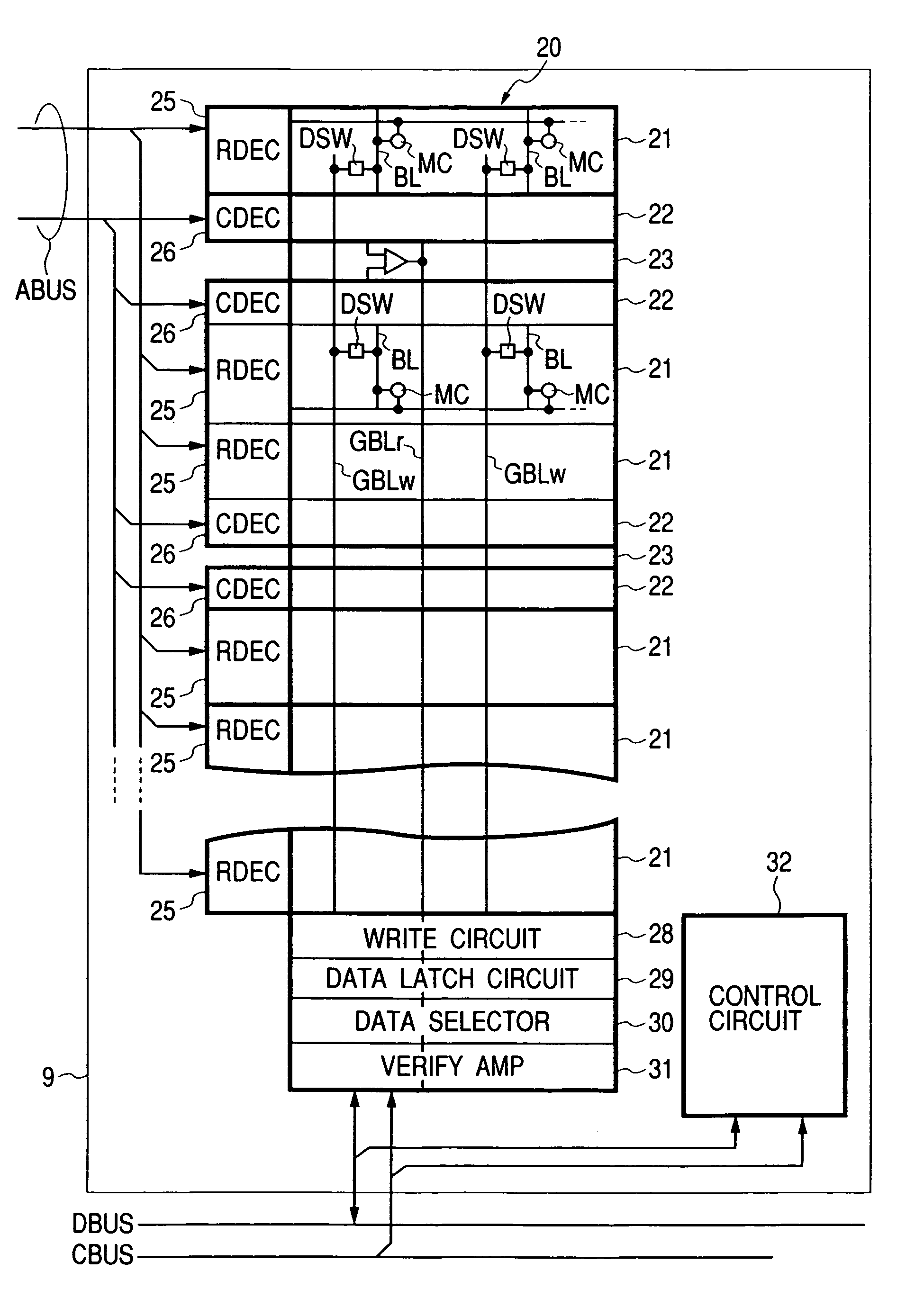
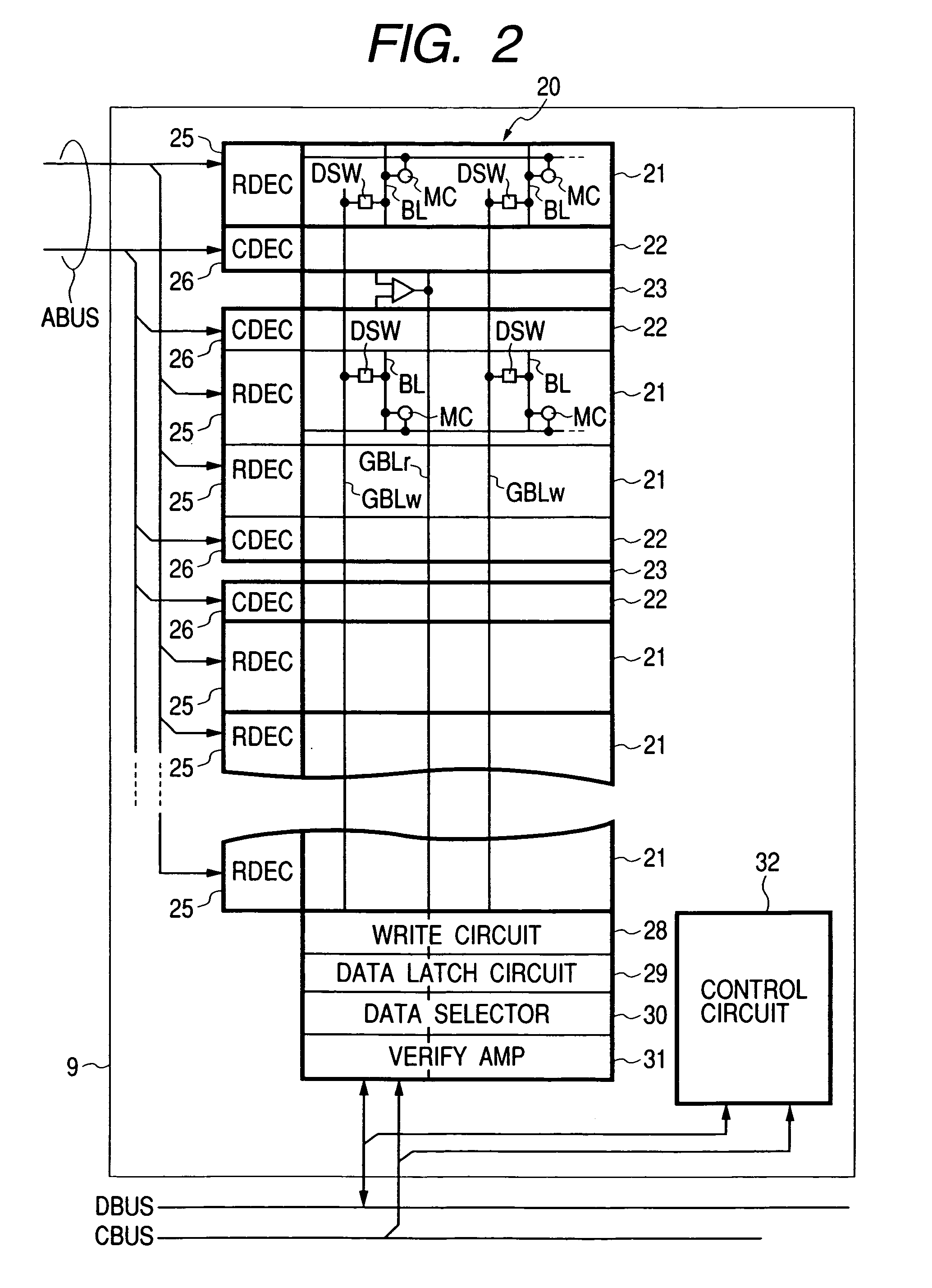
[0067]

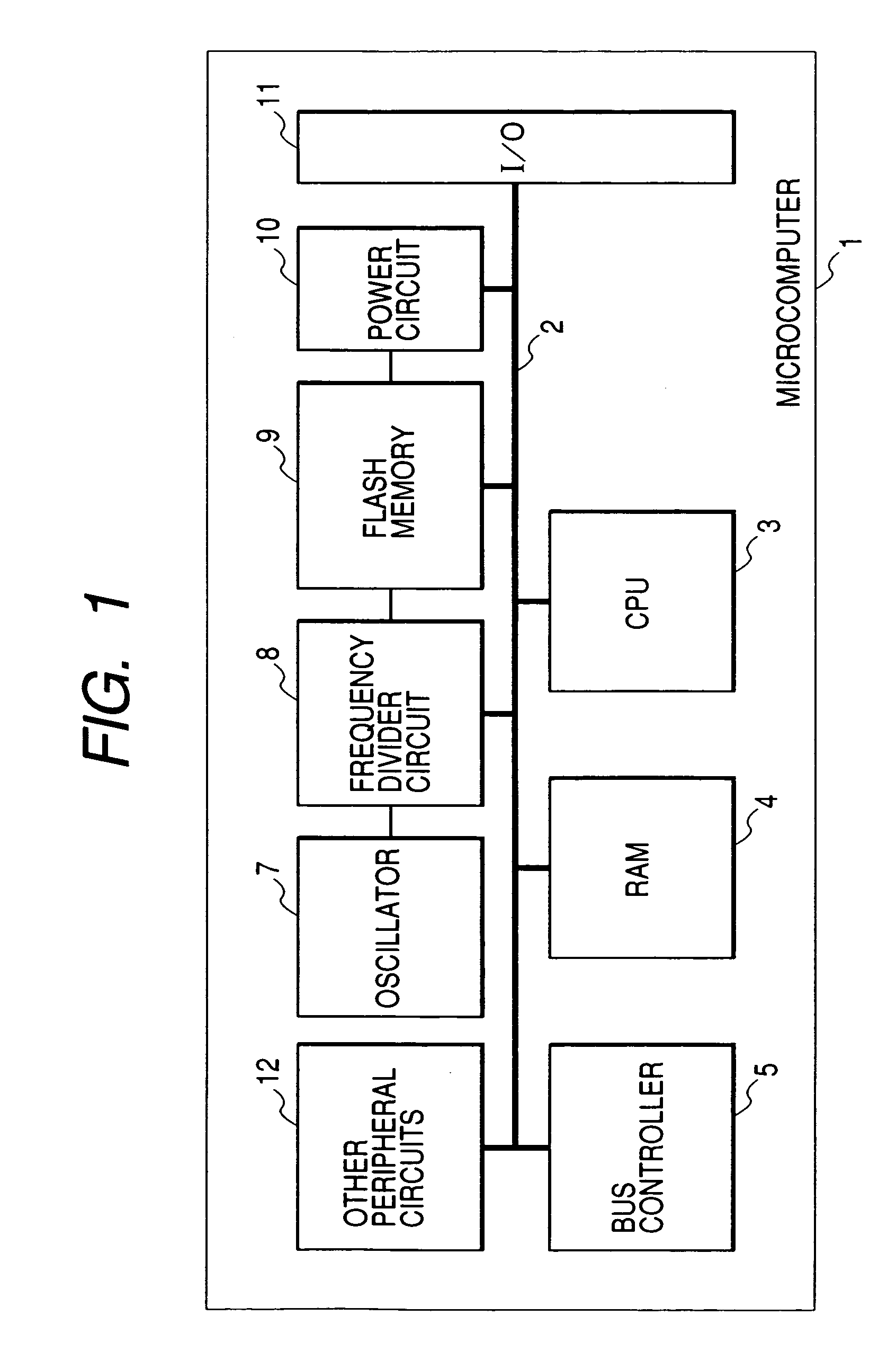
[0068]FIG. 1 illustrates a single-chip microcomputer called a data processor or a microprocessor as an example of a semiconductor integrated circuit according to the present invention.

[0069]The microcomputer shown in the drawing is not particularly limited and is formed over one semiconductor substrate (chip) such as a single crystal silicon by a known semiconductor integrated circuit fabrication technique.

[0070]A microcomputer 1 has, as a circuit module connected to an internal bus 2, a central processing unit (also indicated as a CPU) 3, a random access memory (also indicated as a RAM) 4 used for a work area of the CPU 2, a bus controller 5, an oscillator 7, a frequency divider circuit 8, a flash memory 9, a power circuit 10, an input / output port (I / O) 11, and other peripheral circuits 12 such as a timer counter. The CPU 3 has a command control part and an execution part, decodes a fetched command and performs operation processing by the execution part according to the decod...


PUM


Abstract

The read speed of an on-chip nonvolatile memory enabling electric rewrite is increased. The nonvolatile memory has a hierarchal bit line structure having first bit lines specific to each of a plurality of memory arrays, a second bit line shared between the plurality of memory arrays, a first selector circuit selecting the first bit line for each of the memory arrays to connect the selected first bit line to the second bit line, and a sense amp arranged between the output of the first selector circuit and the second bit line. The hierarchal bit line structure having the divided memory arrays can reduce the input load capacity of the sense amp.

Description

CROSS-REFERENCE TO RELATED APPLICATION[0001]The present application claims priority from Japanese patent application JP 2003-108604 filed on Apr. 14, 2003, the content of which is hereby incorporated by reference into this application.BACKGROUND OF THE INVENTION[0002]The present invention relates to a nonvolatile memory enabling electric erase and write and to a semiconductor integrated circuit such as a data processor called a microcomputer or a microprocessor equipped with the nonvolatile memory together with a central processing unit (also called a CPU), e.g., to a technique effective to be applied to a microcomputer equipped with a flash memory.[0003]In the read operation of a flash memory, 1) a read bit line is precharged, 2) a word line is started up at a selective level such as a high level (“H”) to turn on a memory cell transistor, 3) upon flowing of a memory current via the memory cell transistor, the precharged bit line is drawn out to a low level (“L”), and 4) the potenti...

Claims


Application Information

Patent Timeline
IPC IPC(8): G11C11/34G11C5/06G11C7/18G11C16/06G11C16/02G11C16/04G11C16/08G11C16/26G11C16/28G11C16/30
CPCG11C7/18G11C16/08G11C16/28G11C16/26G11C16/0416G11C2216/22G11C16/30G11C2207/005
Inventor FUJITO, MASAMICHISHINAGAWA, YUTAKASUZUKAWA, KAZUFUMIKAKUDA, AYAKOKATO, AKIRATANAKA, TOSHIHIRO
Owner RENESAS ELECTRONICS CORP
Why Eureka
Try Eureka