Devices related to electrode pads for p-type group iii nitride compound semiconductors

a technology of compound semiconductors and electrode pads, which is applied in the direction of semiconductor devices, semiconductor/solid-state device details, electrical apparatus, etc., can solve the problems of difficult to form the window 20a as planned, difficult to achieve adhesive strength between the au layer and the au layer

Inactive Publication Date: 2002-01-03
TOYODA GOSEI CO LTD
View PDF2 Cites 46 Cited by
  • Summary
  • Abstract
  • Description
  • Claims
  • Application Information

AI Technical Summary

Problems solved by technology

However, because the adhesive strength between the Au layer and the protection layer 20 is weak, e

Method used


Image

  • Devices related to electrode pads for p-type group iii nitride compound semiconductors
  • Devices related to electrode pads for p-type group iii nitride compound semiconductors
  • Devices related to electrode pads for p-type group iii nitride compound semiconductors

Examples


example

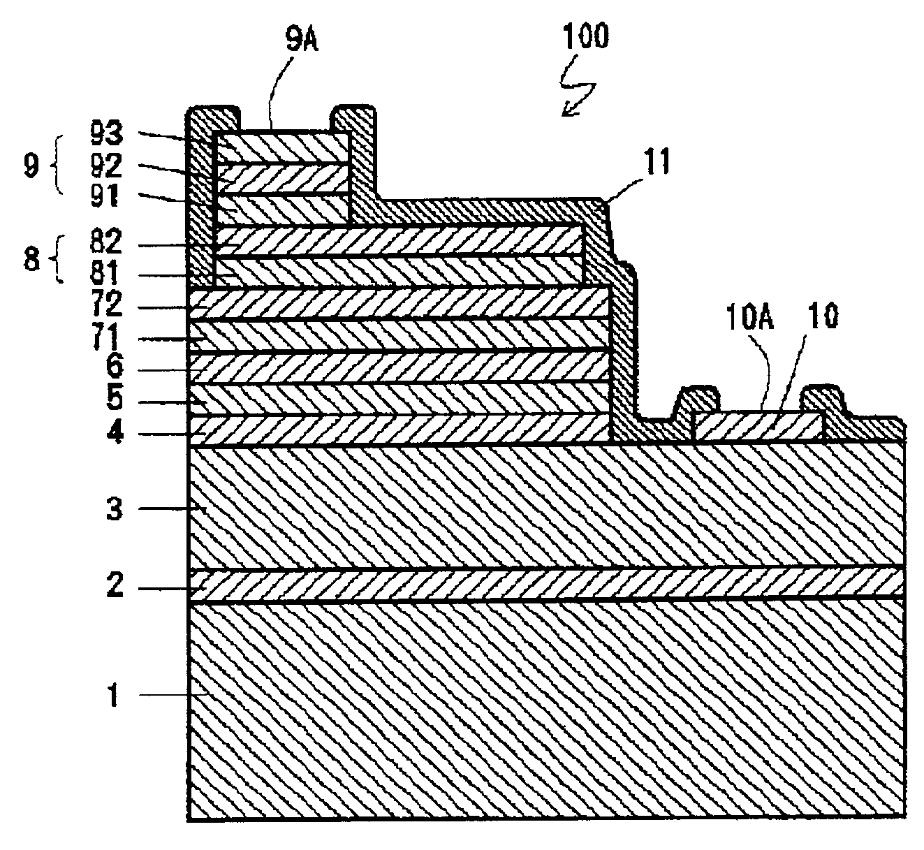
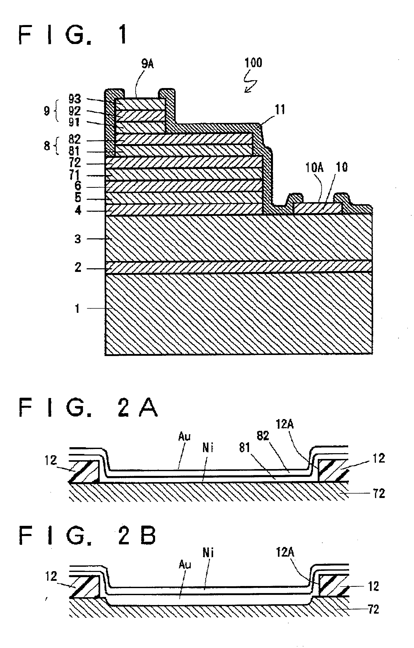
[0033] FIG. 1 shows a sectional view of a light-emitting device 100 made of Group III nitride compound semiconductor which satisfies the formula: Al.sub.xGa.sub.yIn.sub.1-x-yN, wherein 0.ltoreq.x.ltoreq.1, 0.ltoreq.y.ltoreq.1, and 0.ltoreq.x+y.ltoreq.1.

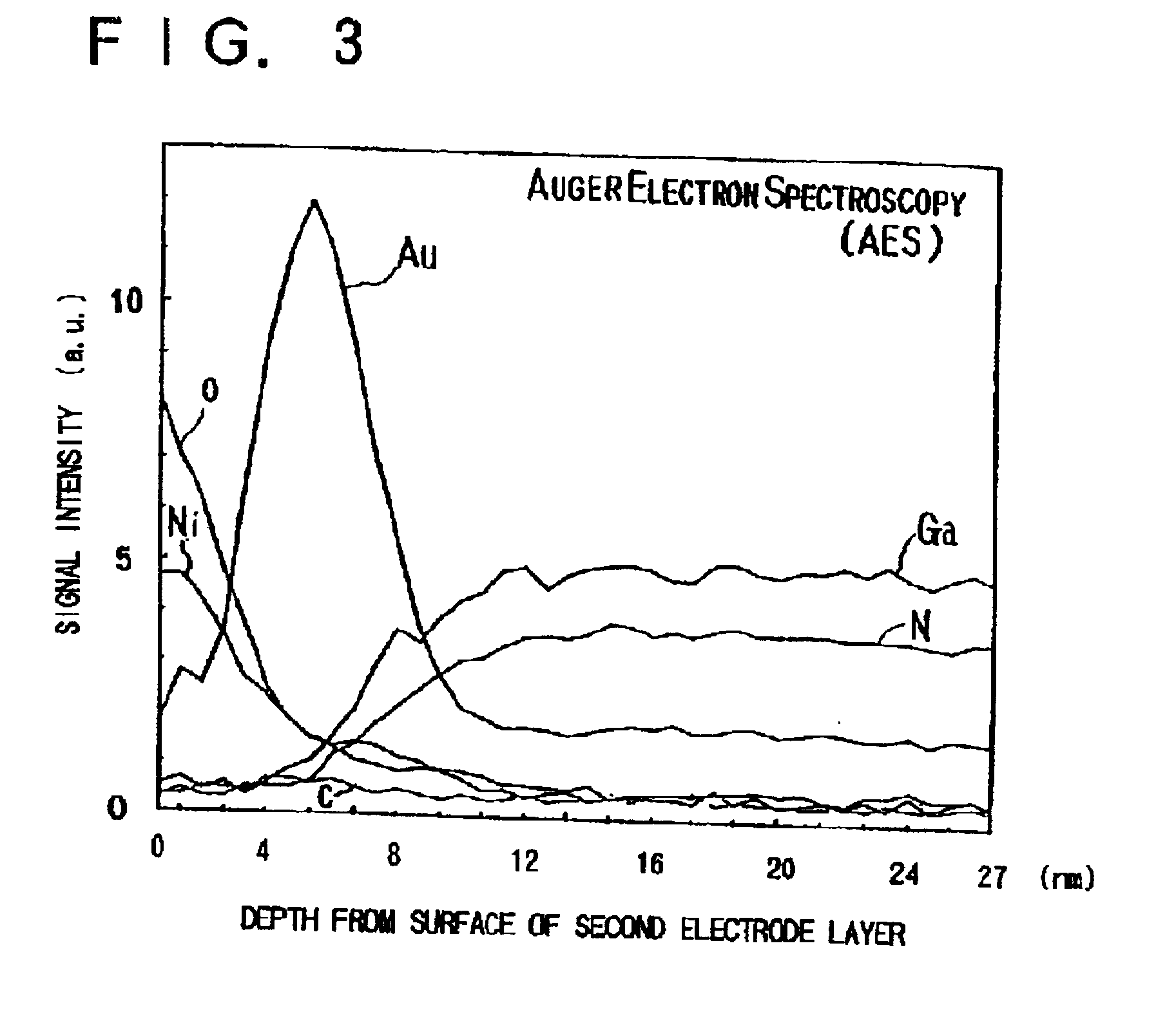
[0034] The device 100 has a sapphire substrate 1. An AlN buffer layer 2 having a thickness generally of 0.05 .mu.m was formed on the sapphire substrate 1. A silicon (Si) doped gallium nitride (GaN) layer 3 of n.sup.+-type, having a thickness generally of 4.0 .mu.m and having an electron concentration of 2.times.10.sup.18 / cm.sup.3, was formed on the AlN buffer layer 2. An Si-doped GaN layer 4, having a thickness generally of 0.5 .mu.m and having an electron concentration of 5.times.10.sup.17 / cm.sup.3, was formed on the n.sup.+-layer 3. A zinc (Zn) and Si doped emission layer 5, comprising of In.sub.0.20Ga.sub.0.80N and having a thickness generally of 100 nm, was formed on the n-layer 4. Respective impurity concentrations of Zn and Si d...


PUM


Abstract

An electrode pad for a Group III nitride compound semiconductor having p-type conduction includes a triple layer structure having first, second, and third metal layers, formed on an electrode layer. A protection film with a window exposing a central portion of the third metal layer is formed by etching on the third metal layer and covers the sides of the first, second, and third metal layers. The second metal layer is made of gold (Au). The first metal layer is made of an element which has ionization potential lower than gold (Au). The third metal is made of an element which has adhesiveness to the protection film stronger than that of gold (Au). Consequently, this structure of the electrode pad improves the adhesive strength between the protection layer and the third meal layer and prevents the etching of the sides of the protection film. Furthermore, the contact resistance between the semiconductor and the electrode pad is lowered and, thus, ohmic characteristic of the electrode pad is improved.

Description

[0001] 1. Field of the Invention[0002] The present invention relates to electrode pads for a Group III nitride compound semiconductor having p-type conduction, a Group III nitride compound semiconductor device having this type of electrode pads, and methods of forming these electrode pads. In particular, the invention relates to electrode pads for a Group III nitride compound semiconductor having p-type conduction with improved adhesive strength and luminous efficiency. Further, the invention relates to a method for forming the electrode pads and preventing the side etching of a protection film when forming a window through the protection film by etching.[0003] 2. Description of Background Information[0004] Conventionally, gold (Au) deposited on a surface of a p-type conductive gallium nitride (GaN) layer is used as an electrode. Because the adhesive strength between the Au layer and the GaN layer is weak, an electrode layer made of Au peels easily away from the GaN layer during all...

Claims


Application Information

Patent Timeline
IPC IPC(8): H01L21/28H01L23/485H01L29/45H01L33/32H01L33/40H01L33/62
CPCH01L24/03H01L24/05H01L24/06H01L29/452H01L2224/05073H01L2224/05155H01L2224/05644H01L2224/05655H01L2924/01002H01L2924/01004H01L2924/01005H01L2924/01006H01L2924/01007H01L2924/0101H01L2924/01012H01L2924/01013H01L2924/01014H01L2924/01015H01L2924/01018H01L2924/01022H01L2924/01025H01L2924/01028H01L2924/01029H01L2924/0103H01L2924/01039H01L2924/01047H01L2924/01049H01L2924/01073H01L2924/01077H01L2924/01078H01L2924/01079H01L2924/01082H01L2924/05042H01L2924/1033H01L2924/3025H01L2924/00014H01L2924/01023H01L2924/01024H01L2924/01033H01L2924/12041H01L2924/12042H01L2924/00
Inventor UEMURA, TOSHIYASHIBATA, NAOKINOIRI, SHIZUYOHORIUCHI, SHIGEMI
Owner TOYODA GOSEI CO LTD
Why Eureka
Try Eureka