Light emitting device

a technology of light emitting device and light source, which is applied in the direction of lighting and heating apparatus, instruments, manufacturing tools, etc., can solve the problems of shortened service life, lowered power output, and changing color balan

Inactive Publication Date: 2002-01-03
TOYODA GOSEI CO LTD +1
View PDF1 Cites 133 Cited by
  • Summary
  • Abstract
  • Description
  • Claims
  • Application Information

AI Technical Summary

Problems solved by technology

This tends to change the color balance over time.
Light emitting elements having poor radiation characteristics can generally cause lowered power output and have ...

Method used


Image

  • Light emitting device
  • Light emitting device
  • Light emitting device

Examples


Embodiment Construction

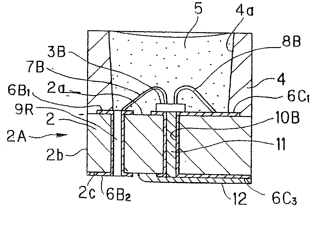
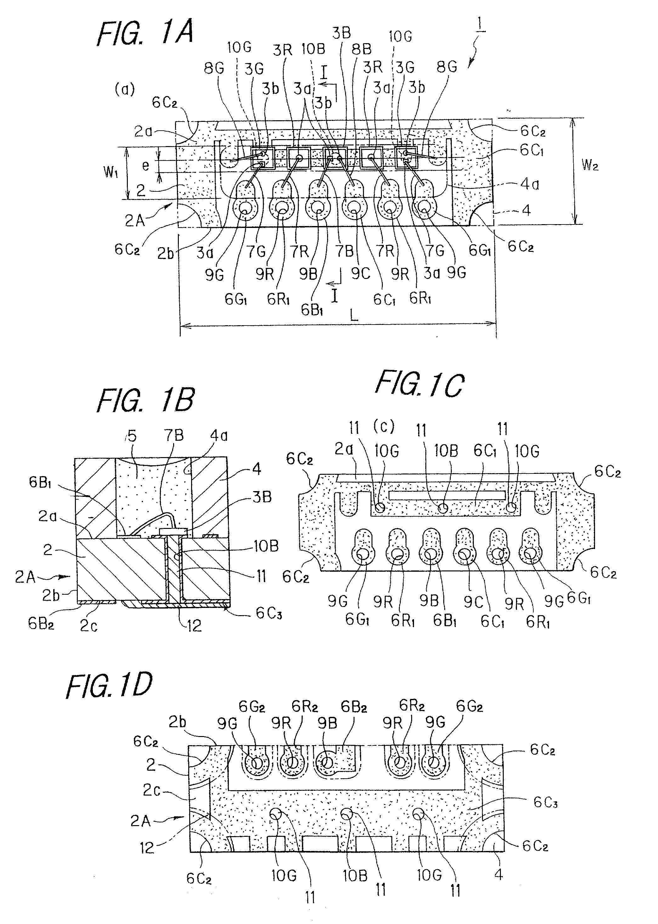
[0041] FIGS. 1A, 1B, 1C and 1D show a light emitting diode or device (LED) in accordance with the principles of the present invention. For the facilitation of understanding, in FIG. 1A, a case and a filling member are not shown, and, in FIG. 1C, a resin is not shown. The light emitting device 1 comprises a printed circuit board 2A on which a metal pattern to be loaded with LED has been printed. A plurality of LEDs 3 (3R (red), 3G (green), 3B (blue)) are disposed in an array. The LED array 3 is electrically connected to the positive and negative leads on the upper surface 2a of the printed circuit board 2A. A case 4 having an opening 4a provided so as to surround the plurality of LEDs 3. A filling member 5, for example, of a transparent epoxy resin, fills the opening 4a and seals the plurality of LEDs 3 in the case 4.

[0042] The printed circuit board 2A includes a base 2 having upper, lower and side surfaces 2a, 2c, 2b, respectively. Preferably, the printed circuit board 2A can be pro...


PUM


Abstract

Separate leads and a common lead are provided on the upper and lower surfaces of a substrate. A plurality of LED elements are disposed in an array on the common lead on the upper surface of the substrate. The common lead provided on the upper surface of the substrate is connected to the common lead provided on the lower surface of the substrate through through-hole plating. Heat generated from the plurality of LED elements is transferred through the common lead provided on the upper surface of the substrate and the through-hole plating to the common lead provided on the lower surface of the substrate and is released therefrom into the air. By virtue of this construction, an light emitting device can be realized in which heat radiating properties are homogenized, heat radiation efficiency is improved, and a compact structure is obtained and, thus, the color balance is improved and unfavorable phenomena such as lowering in the output of light emitting elements and shortening of the service life are avoided.

Description

[0001] This invention is based on Japanese application 2000-165864 filed Jun. 2, 2000, which is hereby incorporated by reference.[0002] 1. Field of the Invention[0003] The present invention relates to a light emitting device, and more particularly to a light emitting device suitable for use, for example, as white light sources for backlight or frontlight in liquid crystal display panels.[0004] 2. Description of Related Art[0005] Various light emitting devices for backlight in full color liquid crystal display panels are known. Generally, a light emitting device (LED) includes an LED chip array comprising an LED for red (R), an LED for green (G); and an LED for blue (B). A light guide section is generally provided such that light from the LED chip array enters therein through an incident face. The light is guided so as to propagate through the inside of the light guide section, thereby permitting planar backlight to be emitted through an outgoing face from the light guide section. Ea...

Claims


Application Information

Patent Timeline
IPC IPC(8): G02F1/1335F21V8/00G02B6/00G02F1/13357H01L33/56H01L33/64
CPCG02B6/0018G02B6/0028G02B6/0051G02B6/0068Y10S362/80H01L2224/48465
Inventor SUEHIRO, YOSHINOBUTAKAHASHI, YUJIKATO, HIDEAKIKAGA, KOICHITESHIMA, KIYOTAKAOHTSUKA, SHUNSUKE
Owner TOYODA GOSEI CO LTD
Why Eureka
Try Eureka