Electronic device and method of driving the same

a technology of electronic devices and electronic devices, applied in the direction of static indicating devices, instruments, solid-state devices, etc., can solve the problems of weak dispersion of electric current characteristics of el drivers, analog methods of gray scale displays,

Inactive Publication Date: 2002-02-28
SEMICON ENERGY LAB CO LTD
View PDF90 Cites 78 Cited by
  • Summary
  • Abstract
  • Description
  • Claims
  • Application Information

AI Technical Summary

Problems solved by technology

An analog method of the gray scale display has a disadvantage in that it is weak with respect to dispersion in the electric current characteristics of the EL driver TFTs.

Method used


Image

  • Electronic device and method of driving the same
  • Electronic device and method of driving the same
  • Electronic device and method of driving the same

Examples


embodiment 1

[0086] Embodiment 1

[0087] Structuring of the memory selection circuit portions in the circuit shown in the embodiment mode using specific transistors, and their operation are explained in embodiment 1.

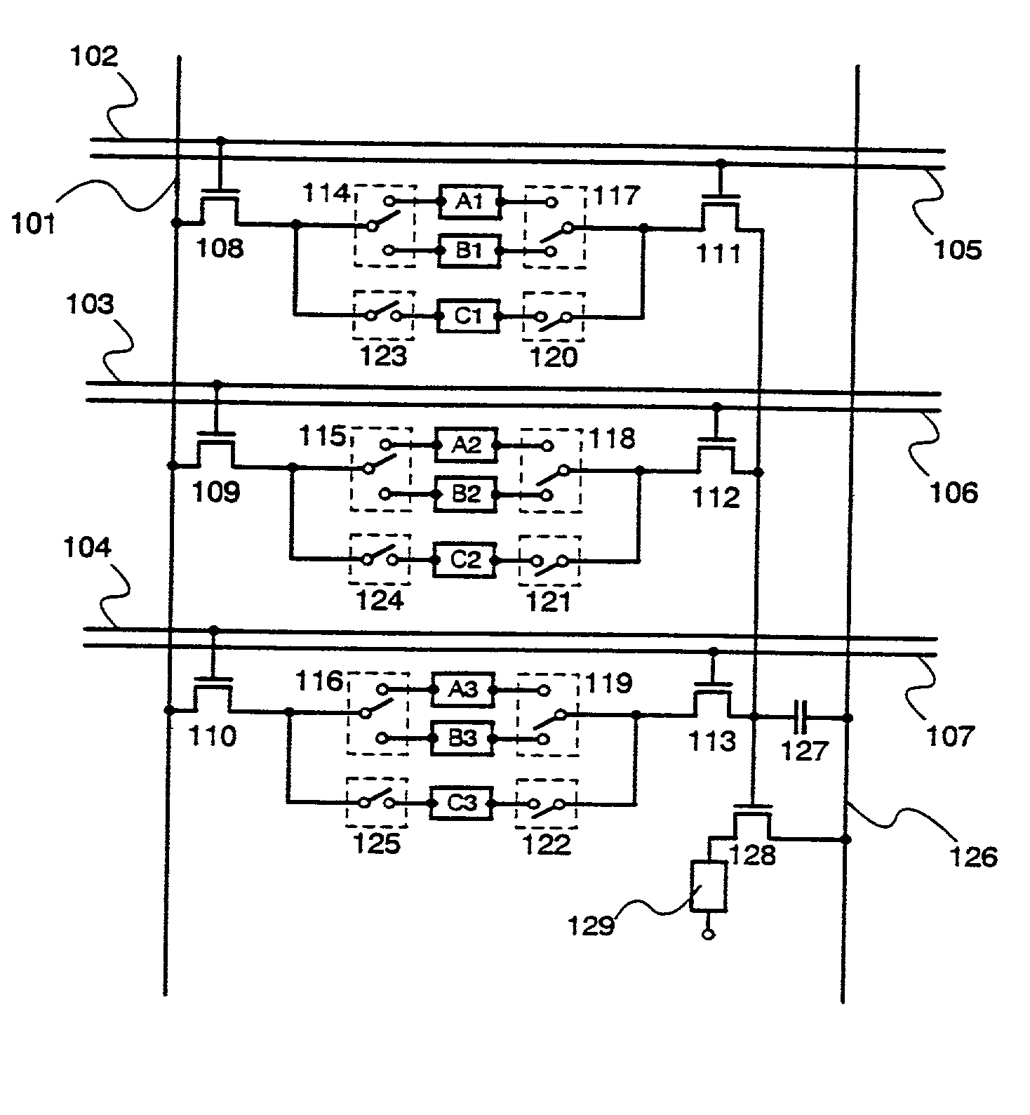
[0088] FIG. 4 is similar to the pixel shown in FIG. 1, and this is an example of structuring the periphery of the memory circuit selection portions with actual circuits. Within FIG. 4: write-in selection TFTs 420, 422, 424, 426, 428, and 430; and read-out selection TFTs 421, 423, 425, 427, 429, and 431 are formed in each of the volatile memory circuits A1 to A3, and B1 to B3. Control is performed using memory circuit selection signal lines 414 to 419. Write-in selection TFTs 435, 437, and 439, and read-out selection TFTs 436, 438, and 440 are formed in each of the non-volatile memory circuits C1 to C3, and control is performed using memory circuit selection signal lines 432 to 434, and 441 to 443. The pixel shown in embodiment 1 is one in which two frame portions of a 3-bit digital ima...

embodiment 2

[0105] Embodiment 2

[0106] An example in which a second latch circuit is omitted from a source signal line driver circuit by performing write-in to memory circuits of a pixel portion point by point is discussed in embodiment 2.

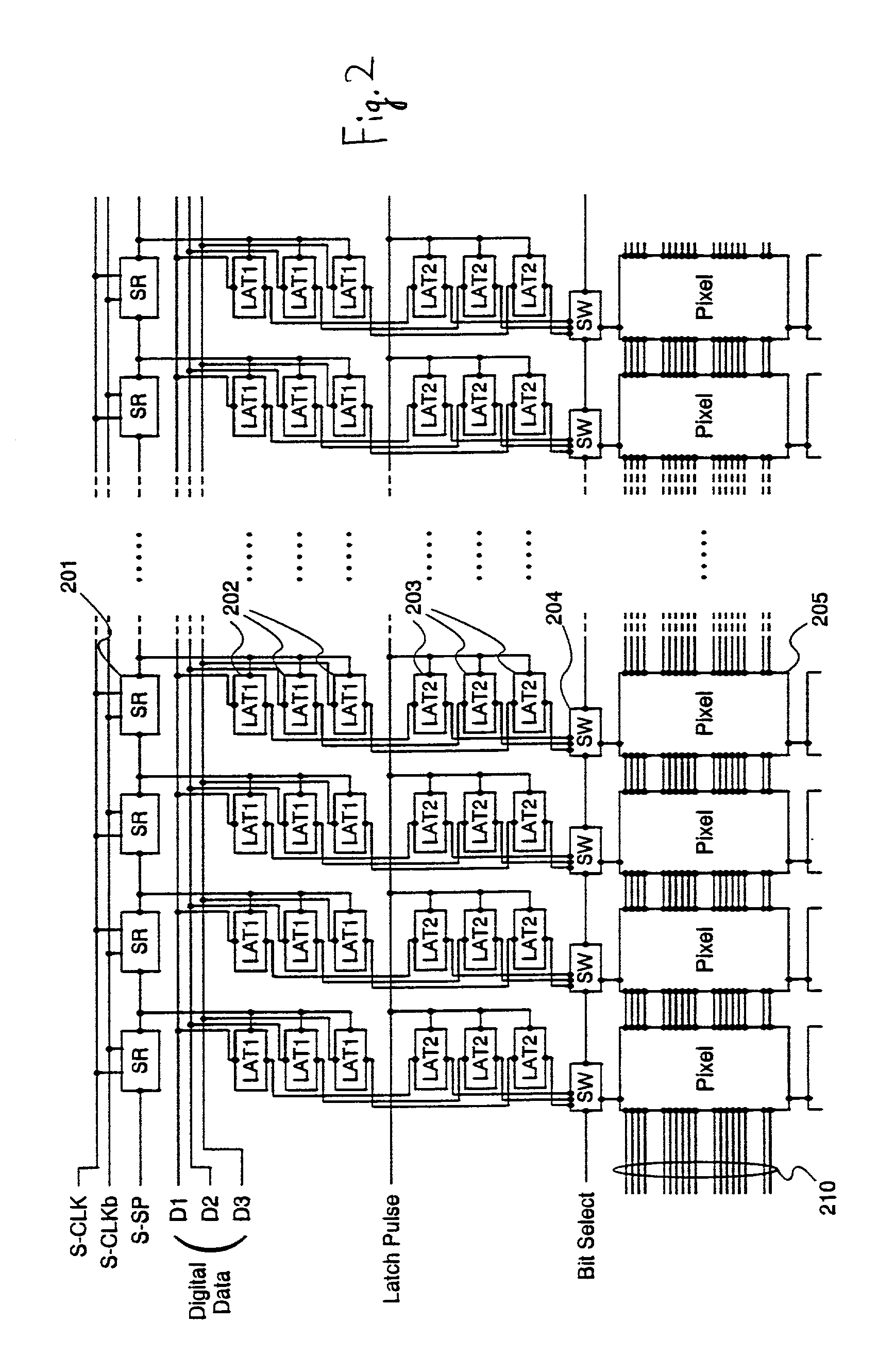
[0107] FIG. 5 shows a structure of a source signal line driver circuit and a portion of a pixel in an electronic device using a pixel having memory circuits. This circuit corresponds to a 3-bit digital gray scale signal, and has a shift register circuit 501, a latch circuit 502, and a pixel 503. Reference numeral 510 denotes a signal line to which a signal supplied from a gate signal line driver circuit, or supplied directly from outside, is input, and its explanation, along with that of the pixel, is given later.

[0108] FIG. 6 is a detailed diagram of a circuit structure of the pixel 503 shown in FIG. 5. Similar to embodiment 1, this corresponds to 3-bit digital gray scales, and has an EL element 646, a storage capacitor 644, volatile memory circuits (A1 to A3,...

embodiment 3

[0120] Embodiment 3

[0121] An example of an electronic device using a method in which write-in to memory circuits within a pixel is performed by line-sequential drive is discussed in embodiment 3. The circuit structure of the electronic device in embodiment 3 corresponds to that shown in embodiment 2, in which the second latch circuit is omitted.

[0122] FIG. 17 shows an example circuit structure of a source signal line driver circuit of the electronic device shown in embodiment 3. The circuit here corresponds to a 3-bit digital gray scale signal, and has a shift register circuit 1701, latch circuits 1702, switching circuits 1703, and pixels 1704. Reference numeral 1710 denotes a signal line into which a signal supplied from a gate signal line driver circuit, or directly from the outside, is input. The circuit structure of the pixel may be similar to that of embodiment 2, and therefore FIG. 6 may be referenced as is.

[0123] FIGS. 18A to 18C are timing charts relating to operation of the...


PUM


Abstract

In an electro-optical device for performing image display using an n-bit (where n is a natural number, n>=2) digital image signal, nxm (where m is a natural number) volatile memory circuits, and nxk (where k is a natural number) non-volatile memory circuits are contained in every one pixel. The electro-optical device has a function for storing m frame portions of the digital image signal in the volatile memory circuits, and k frame portions of the digital image signal in the non-volatile memory circuits. By performing display of a static image in accordance with repeatedly reading out, for each frame, the digital image signal stored once in the memory circuits and performing display, drive of a source signal line driver circuit can be stopped during that period. Further, a digital image signal stored in the non-volatile memory circuits is stored even after a power source is cut off, and therefore display is possible immediately when the power source is next turned on.

Description

[0001] 1. Field of the Invention[0002] The present invention relates to an electronic device and a method of driving an electronic device. In particular, the present invention relates to an active matrix electronic device having thin film transistors formed on an insulator, and to an active matrix electronic device using the method of driving an electronic device. Among such devices, the present invention relates to an active matrix device using a digital image signal as an image source and using a self light emitting element such as an organic electro luminescence (EL) element (a light emitting diode or OLED (Organic Light Emission Diode)) in a pixel portion, and to an active matrix electronic device using the method of driving. The EL devices referred to in this specification include triplet-based light emission devices and / or singlet-based light emission devices, for example.[0003] 2. Description of the Related Art[0004] The spread of electronic devices having a semiconductor thi...

Claims


Application Information

Patent Timeline
Patent Type & Authority Applications(United States)
IPC IPC(8): G09G3/20G09G3/32H01L27/15
CPCG09G3/2018G09G3/2022G09G3/3266G09G3/3275G09G2300/0809G09G2300/0842G09G2300/0857G09G2300/0861G09G2330/021G09G2360/18
Inventor KOYAMA, JUNYAMAZAKI, SHUNPEI
Owner SEMICON ENERGY LAB CO LTD
Why Eureka
Try Eureka