Method for polishing leads for semiconductor packages

a technology for semiconductor packages and polishing methods, which is applied in the direction of carpet cleaning, vehicle cleaning, bowling games, etc., can solve the problems of difficult to precisely polish the leads, difficult to polish the leads without any damage, and long polishing process

Inactive Publication Date: 2002-03-21
LAPIS SEMICON CO LTD
View PDF0 Cites 9 Cited by
  • Summary
  • Abstract
  • Description
  • Claims
  • Application Information

AI Technical Summary

Benefits of technology

[0005] Accordingly, an object of the invention is to provide a method by which leads of a semiconductor package can be polished efficiently and precisely.
[0006] Another object of the invention is to provide an apparatus, which polishes leads of a semiconductor package efficiently and precisely.

Problems solved by technology

According to the conventional way, however, the polishing process takes a long period of time, and it is difficult to polish the leads without any damages, such as bent and break thereon.
Further, it is difficult to polish the leads precisely to provide enough contact-reliablity.

Method used


Image

  • Method for polishing leads for semiconductor packages
  • Method for polishing leads for semiconductor packages
  • Method for polishing leads for semiconductor packages

Examples


Embodiment Construction

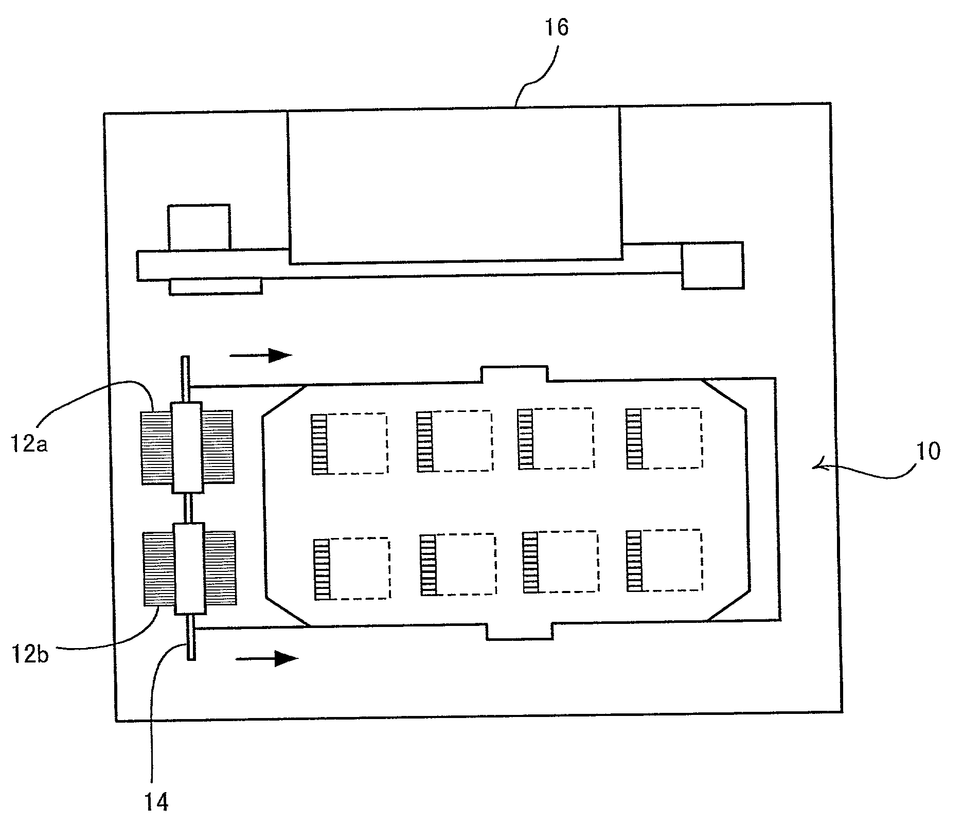
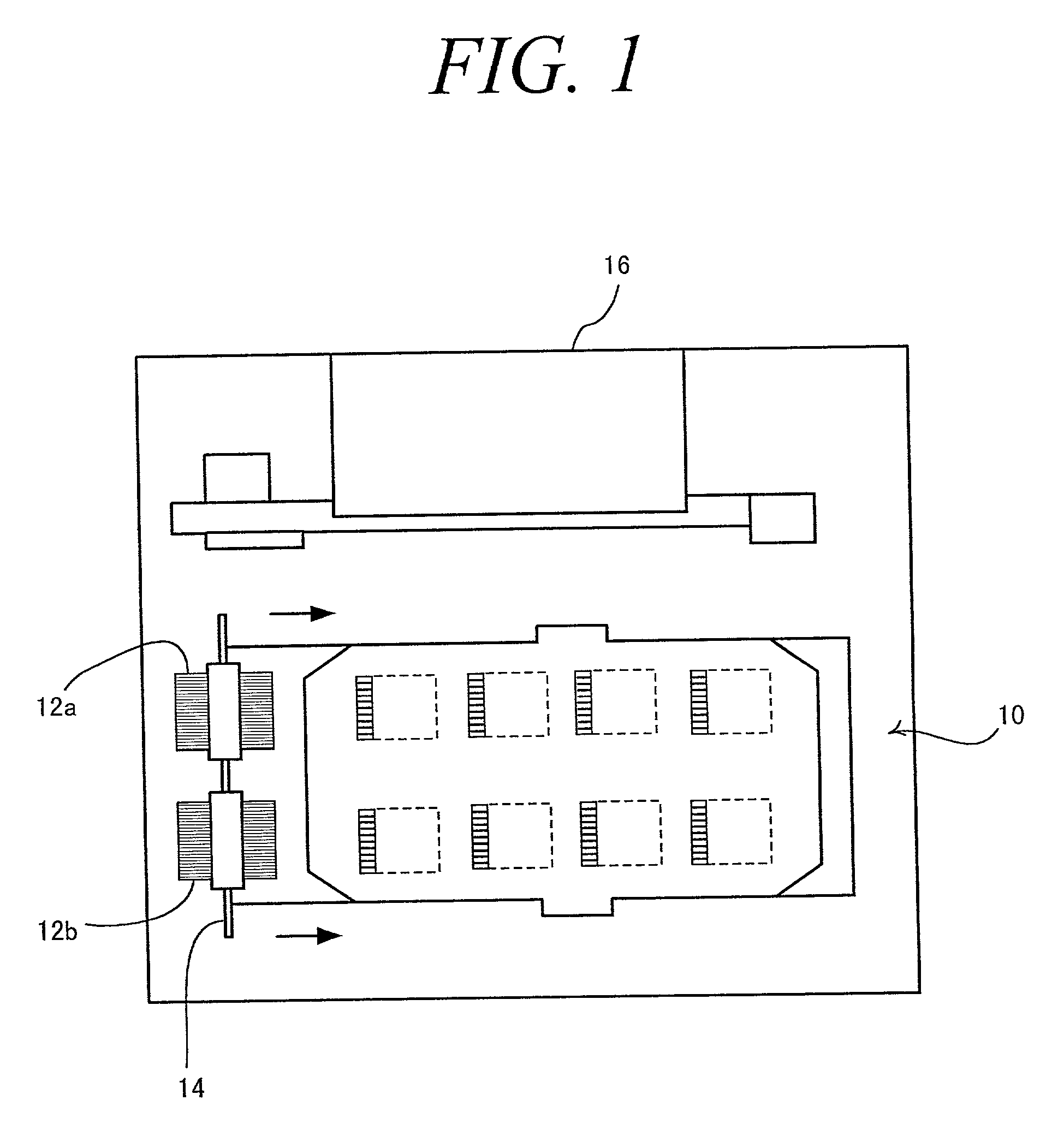
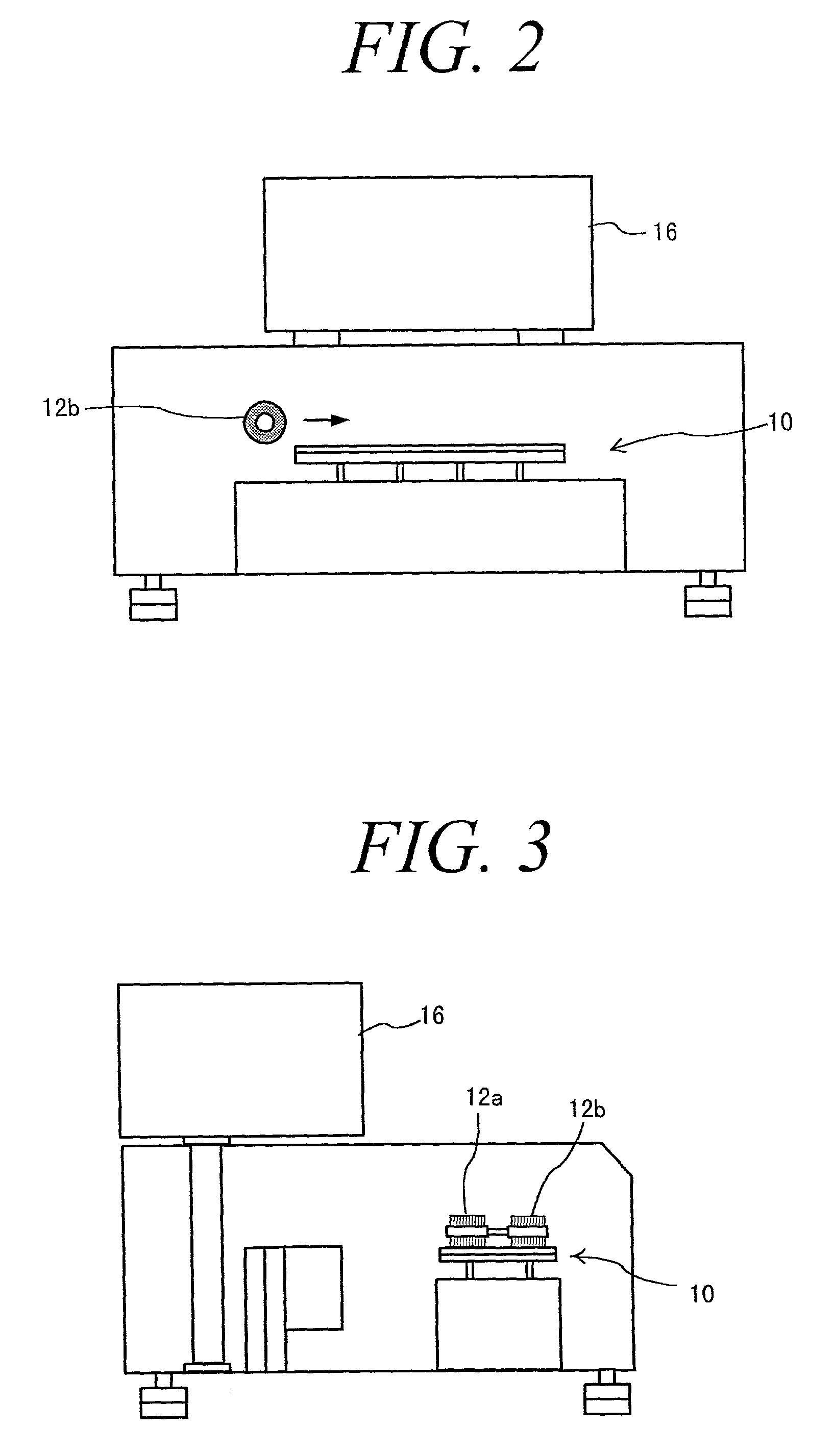
[0021] FIGS. 1, 2 and 3 show a polishing apparatus, according to an embodiment of the invention, which automatically polishes leads of LSI packages. The polishing apparatus includes a package holder unit 10, a pair of wire brushes 12a and 12b, a shaft 14 and a control unit 16. The package holder unit 10 is designed to hold eight LSI packages on it. The wire brushes 12a and 12b are rotatably provided on the shaft 14, and are designed to move both in vertical and horizontal directions over the package holder unit 10. The wire brushes 12a and 12b may be made of stainless steel or brass. The control unit 16 controls the package holder unit 10 and the wire brushes 12a and 12b so that the leads of LSI packages are well polished.

[0022] FIGS. 4 and 5 show the structure of the package holder unit 10. The package holder unit 10 includes a base frame 20, a clamp plate 22, a mask 24 and eight package holders 26. The base frame 20 is composed of two pieces of frame members and is arranged at the...


PUM

PropertyMeasurementUnit
rotation speedaaaaaaaaaa
pressureaaaaaaaaaa
timeaaaaaaaaaa

Abstract

In a method for polishing leads of a semiconductor package, a plurality of semiconductor packages is arranged in a certain manner. Then, the leads are automatically polished. The semiconductor packages may be masked to expose at least a part of the leads to be polished.

Description

[0001] This application claims the priority of Application No. H09-243709, fled Sep. 9, 1997 in Japan, the subject matter of which is incorporated herein by reference.[0002] The present invention relates to technology for polishing leads of a semiconductor package, such as an LSI package. And more particularly, the invention relates to a method and an apparatus for polishing leads, which contribute to improve the reliability of a semiconductor package.[0003] In semiconductor fabrication processes, a semiconductor package is formed to protect an LSI chip contained therein. To improve the quality of a surface-mounting type of semiconductor package, it is important to make leads to have good contact-reliability.[0004] Conventionally, the leads of an LSI package are manually polished with a brush, or the like. According to the conventional way, however, the polishing process takes a long period of time, and it is difficult to polish the leads without any damages, such as bent and break ...

Claims


Application Information

Patent Timeline
Patent Type & Authority Applications(United States)
IPC IPC(8): B24B29/02H01L21/48H01L23/50B24B29/00
CPCB24B29/005Y10T29/49121H01L21/4835B24B29/02
Inventor SATO, TAKEYUKI
Owner LAPIS SEMICON CO LTD
Why Eureka
Try Eureka